This thread has been locked.

If you have a related question, please click the "Ask a related question" button in the top right corner. The newly created question will be automatically linked to this question.

OPA552: Design causing high frequency noise at op amp output

Part Number: OPA552
Other Parts Discussed in Thread: TINA-TI

Hello,

I'm working on a design revision for a circuit that uses the OPA552. I have a few questions I'd like to resolve to understand why our current design might be flawed. We are seeing a lot of high frequency noise at the output signal of the op amps.

1. After reading the datasheet on page 1, I see that this op amp is optimized for gains of 5 or greater. In our application, we have circuits where the OPA552 has gains of 1 and 2. In these designs, we are seeing a lot of high frequency noise at the output of the op amp. Does "optimized" mean that the op amp is unstable for gains below 5? Would you expect to see this high frequency noise as a result of using the low gains?

2. I see that the op amp has three V- pins in the SOIC-8 version (pins 1, 4, and 5). On page 17 of the datasheet, there is a note that pins 1 and 5 should not be attached to the negative power supply and should not be used as current carriers for the SOIC-8. Does this note only apply when V- is connected to a negative power supply or also when V- is grounded? We have the op amp in our application running with 24 V at V+ and V- is grounded. I'm thinking this could also be a cause of our issues. The datasheet mentions to expect performance reductions when doing this. What kind of performance reductions can be expected? Would this cause high frequency noise? I also disconnected pins 1 and 5 from ground and retested to find the high frequency noise still there. Could doing that have caused permanent damage to the chip, or is this a sign that this is not the root cause of the issue?

Any help would be much appreciated.

Sincerely,

Mike

  • Mike,

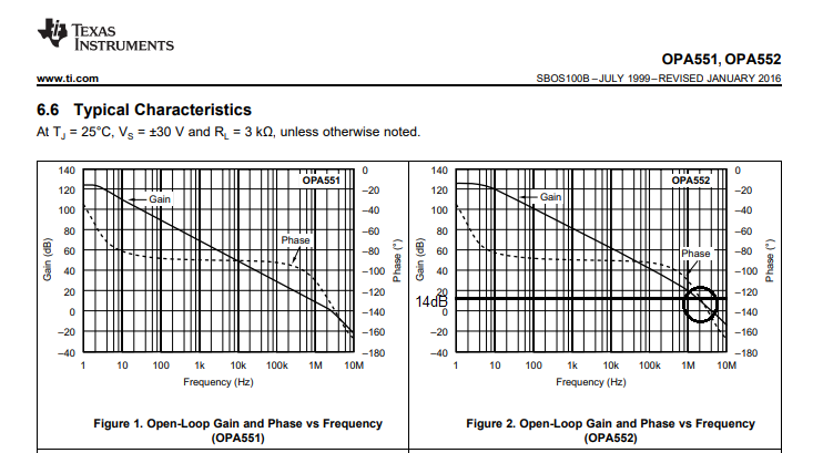
    OPA552 is a decompensated op amp requiring a minimum gain of G>5 (14dB) to be stable - see below.  For AC<5 phase margin is below 45 degrees and the circuit may oscillate.

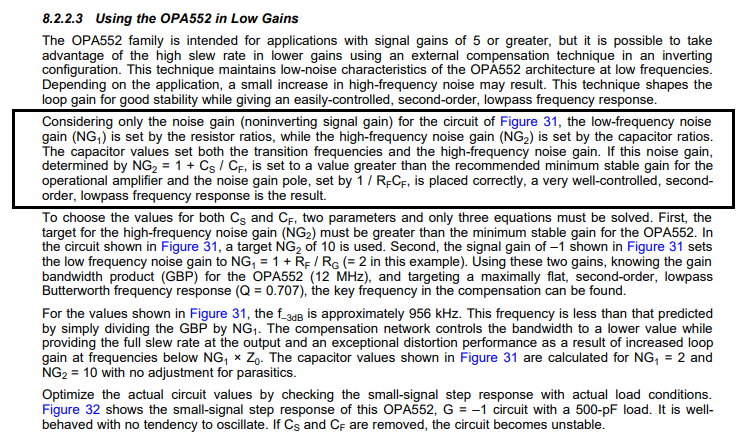
    There is a way to stabilize the circuit for lower DC gains (controlled by rationing of resistors) by increasing the AC gain  (controlled by rationing of capacitors)

    - read below.  Even though SOIC diagram shows pin 1 and 5 as (V-), in fact I believe they are all No Connect (NC) and should have to effect on the noise level you see. 

  • Marek,

    Thanks for your reply. That is helpful. That makes sense for why we were seeing the oscillations. Just so that I understand how this works correctly, why does a phase margin less than 45 degrees indicate that the circuit may oscillate?

    Your second comment makes sense. I didn't see any change between when the pins were connected vs. not in the noise. 

    Mike

  • Mike,

    In order to assure stability of the circuit over wafer fab process variations, we recommend designing the system for the minimum phase margin (PM) of 45 degrees so over process, temperature, power supply, etc. variation the system does not become unstable. For the gain of 5 OPA552 meets the minimum PM of 45 degrees and thus is stable BUT for gains of 1 or 2 you use its phase margin is less than 45 degrees, which is the reason you see oscillation.

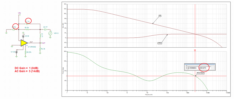
    There is a way to increase the AC gain to make the circuit stable without increasing DC gain - see example below showing 68 degrees phase margin.

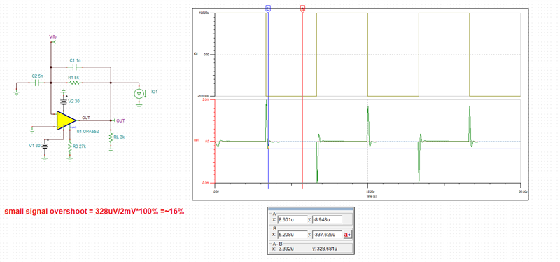
    The stability of the circuit may be confirmed by transient analysis showing 16% small-signaovershoot whereas the maximum recommended is 25%.

    Please review the Stability material under following link- https://www.ti.com/video/series/precision-labs/ti-precision-labs-op-amps.html

    Below I have attached Tina-TI schematics for your convenience.

    OPA552 AC Stabiity.TSC

    OPA552 Transient Stabiity.TSC

  • Thanks, Marek. I appreciate your help. I know what I need to do going forward.