Part Number: JFE150
Other Parts Discussed in Thread: JFE2140, OPA202, , OPA210, OPA197
Hello,
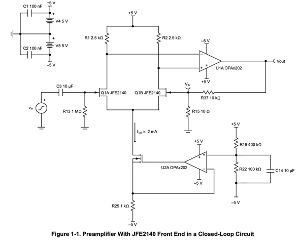
I would like to modify the JFE2140 preamplifier design (uses the JFE2140 and OPA202) that is a really great design.
This thread has been locked.
If you have a related question, please click the "Ask a related question" button in the top right corner. The newly created question will be automatically linked to this question.
Hey Adam,
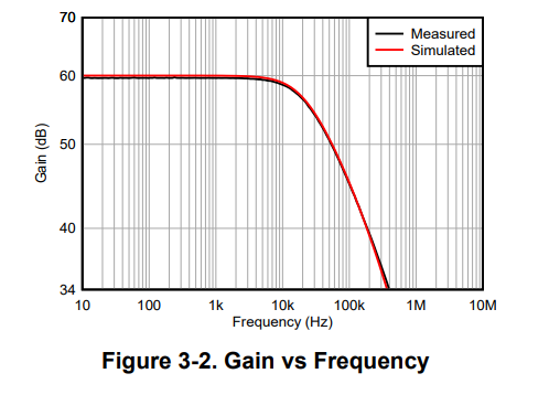
Thank you for the compliments on my work! The gain decrease from 60 dB to 26 dB has the benefit of creating more bandwidth of the overall circuit. The closed loop bandwidth (Acl) has a -3 dB point that occurs when Aol and 1/beta intersect. In the mid-band frequencies Acl follows 1/beta. When 1/beta is lowered in gain the intersection of Aol and 1/beta occurs at a higher frequency thus extending the closed loop bandwidth. This can be seen visually below.
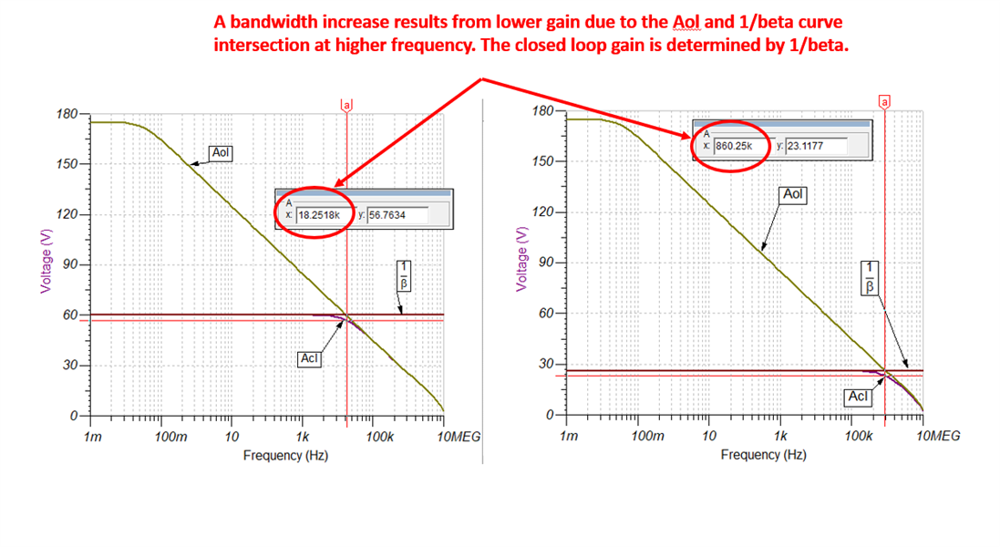
Note that this circuit has a flat closed loop response extending down to 1 mHz. This is actually one of the nice trade offs between this design and the JFE150 design where large capacitors are needed to achieve such a low linear response.
I measured down to 10 Hz flat on the EVM. I went to 10 Hz due to measurement limitation.
To bandwidth limit the closed loop response a capacitor can be placed in the feed-forward Aol circuit. Specifically on the OPA202 feedback path or whatever amp is chosen for the composite amplifier. This is shown below. I chose 500 pF for my example. This causes the Aol curve to drop sooner and therefore the intersection of the Aol and 1/beta curves occur sooner. Note that in order to change the gain to 26 dB the feedback resistor in the beta network is changed from 10 k to 189.5 ohms below.
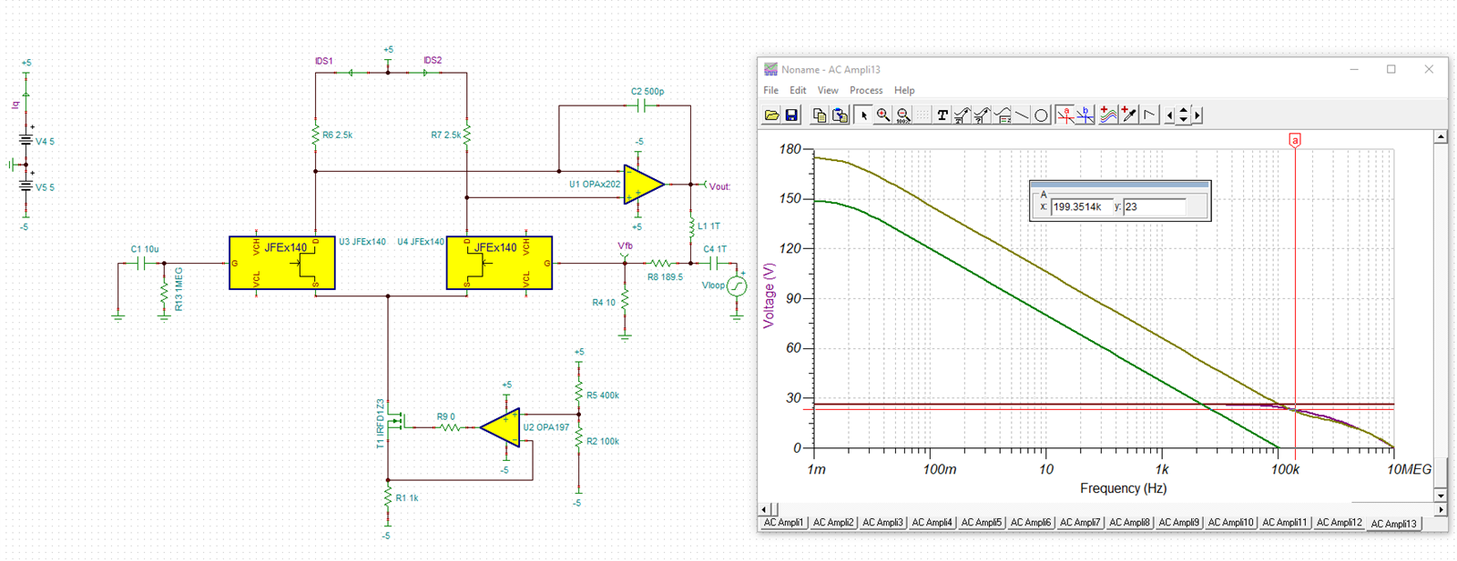
A quick spot check shows that the circuit is still stable. Applying a step such that the output is exercised by 10 mV I observe no ringing.
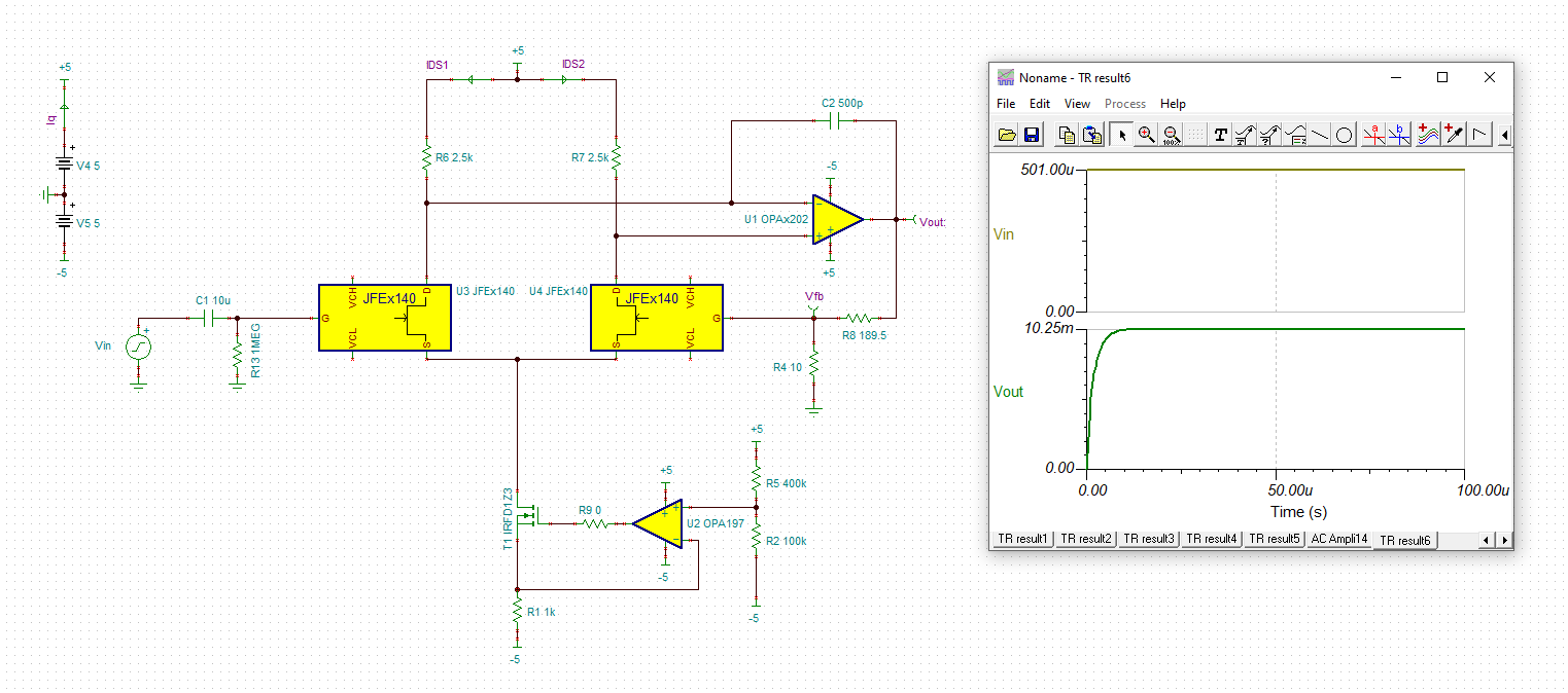
I hope this helps clarify! I have attached my Tina simulations below. Let me know if you have any further questions.
JFE2140 Loop Parameters.TSCJFE2140 Stability check.TSC
Best Regards,
Chris Featherstone
Hi Chris,
Thanks for your response. It looks like that will do what I need then.
Thanks!
Hey Adam,
The input capacitance of the JFET is very low and an order of magnitude lower than the sensor capacitance. I don't think this will be an issue. The input impedance of the JFET is very high and I don't see this creating an issue with the input device you described.
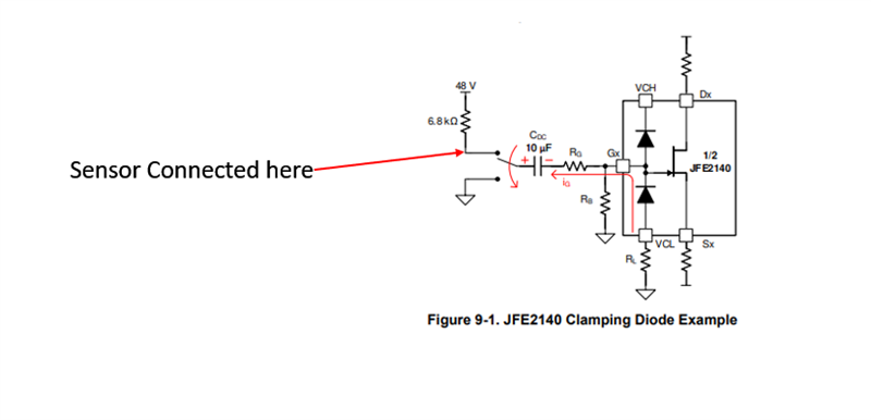
Are you wanting to use the 48 V phantom power to power the JFET and the input device?
For a single ended in phantom power connection the example below could be used:
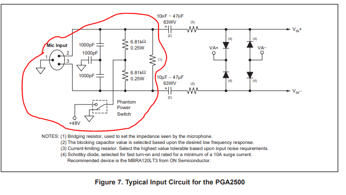
For a differential in, the front end example below could be used:
Best Regards,
Chris Featherstone
Hi Chris,
Do you think sticking with the OPA202 then is best with lower noise? It seems there is not a lot of noise generated from the OPA202 when I ran your TINA model with a noise analysis
Thank you
Hey Adam,
Yeah the OPA202 is very low noise due to it being a bipolar input. The OPA202 and OPA210 are both bipolar inputs. The difference is going to come down to the noise vs power consumption. Note that that the Iq of the devices are different. The OPA210 has higher Iq but also has lower noise. This will be the main trade off consideration. If power consumption isn't a big concern then the OPA210 would certainly be a good candidate for the composite amplifier. The input referred noise is divided from the output by the overall gain of the circuit back to the JFET front end. This is a nice benefit of this circuit. The JFET provides low noise and high input impedance and can be used to replace the front end of the bipolar input stage of the op amp. The JFET provides it's own gain via gm prior to the op amp. It's a best of both worlds scenario where you get the noise benefit of a bipolar amp but also high input impedance with flexible biasing and gain from the JFET.
Best Regards,
Chris Featherstone
Thanks Chris, that makes sense. Also, I notice in your TSC files you used the OPA197 on one part of the circuit- did you mean for that to be the OPA202? I think so, but wanted to confirm. Thank you for all the insight.
Hey Adam,
No problem! Let me know if you have any further questions. I think I was deciding on the amplifier to put on the EVM at the time and this was one of my older revision Tina files. I ended up using the OPA202 on the EVM in both locations. I wanted to demonstrate that you can use a bipolar amp for a sensor with high source impedance by replacing the front end of the bipolar amp with a high input impedance JFET front end and benefit from the noise performance. To keep things consistent I ended up settling with the OPA202 in both locations. The noise seen at both sources of the dual JFET pair is seen as a common mode signal.
Best Regards,
Chris Featherstone