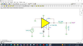
Below INA159 schematic snapshot and connection.
There are two options set for Vref between 0V to 2.5V by mounting R23 and R24 resistors.
I have query that in first option where R23 is mounted and R24 IS Do not populate. At that scenario 1 theoretically output voltage value is going to negative side but in simulation it is value around 1.96mV.
There is any ASIC design inside the opamp INA159 that will give as per below simulated values. Circuit also shown below for reference. At +IN pin applied voltage and -IN pin is grounded in both scenarios.
In second scenario theoretical and simulated value is perfectly matched. Could you please guide me on that why simulated value is different from calculated values? INA159 Simulated reading.xlsx
| Applied Voltage @ +IN,-IN (V) |
Voltage @ Vout | Theoritical Vout(V) | Applied Voltage @ +IN,-IN |
Voltage @ Vout | Theoritical Vout(V) | 2.5 | |||
| 10 | 1.999997V | 2 | 10 | 4.500011V | 4.5 | ||||
| 2.5 | 499.989673mV | 0.5 | 2.5 | 3.000003V | 3 | ||||
| 1 | 199.98811mV | 0.2 | 1 | 2.700001V | 2.7 | ||||
| 0.2 | 39.989347mV | 0.04 | 0.5 | 2.600001V | 2.6 | ||||
| 0.1 | 19.993115mV | 0.02 | 0.1 | 2.520003V | 2.52 | ||||
| -0.1 | 1.965223mV | -0.02 | -0.1 | 2.480001V | 2.48 | ||||
| -0.2 | 1.941491mV | -0.04 | -0.5 | 2.400002V | 2.4 | ||||
| -1 | 1.967217mV | -0.2 | -1 | 2.299999V | 2.3 | ||||
| -2.5 | 1.957365mV | -0.5 | -2.5 | 1.999997V | 2 | ||||
| -10 | 1.954625mV | -2 | -10 | 499.989673mV | 0.5 | ||||
| Table1 | Table2 | In Table 2 R23 DNP and R24 mounted. |


 Scenario 1
 Scenario2
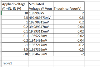 Scenario 1
 Scenario 2


 Scenario1
 Scenario2