This thread has been locked.

If you have a related question, please click the "Ask a related question" button in the top right corner. The newly created question will be automatically linked to this question.

LMH6401EVM: Step response over-damped

Part Number: LMH6401EVM
Other Parts Discussed in Thread: LMH6401, OPA855DSGEVM, OPA855

Hi there,

I was trying to test the LMH6401EVM output with the square wave input.

As shown in the figure below, the green and purple channels are the differential inputs (positive and negative).

The yellow and blue channels are the outputs. It seems that the step response is over-damped.
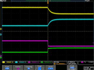
The DC power input is +-2.4V.

My question is how to obtain the critically-damped response?

Can we change some resistor and capacitor values to realize this? Any model can be used for simulation?

Thanks and best,

Yilun

  • Hi Yilun,

    Thank you for providing the oscilloscope plot. I do have a few additional questions:

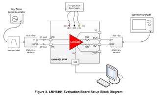
    • Are you testing the LMH6401EVM using the following setup, as shown in the user's guide?

    • What are the magnitude and frequency of the square wave input that you are using (it is hard to read from the plot you have provided)?
    • What output voltage is being observed and what is the rise time of the step response you are observing?
    • What gain are you setting the LMH6401 to operate in?

    Also, I have attached a simulation file that should match closely to the test setup of the LMH6401EVM.

    LMH6401_E2E.TSC

    Thanks,

    Nick

  • Hi Nick,

    Please see my response below:

    1. "Are you testing the LMH6401EVM using the following setup, as shown in the user's guide?"

    The setup is similar. The VIN+ and VIN- for my setup are the differential outputs from an FPGA (Xilinx ZCU216). I connected OUT+ and OUT- directly to the scope. I didn't connect the USB, so the variable attenuation should be the default value (I guess the attenuation is 32 dB for default?).

    2. "What are the magnitude and frequency of the square wave input that you are using (it is hard to read from the plot you have provided)?"

    400 mV, 3.9 kHz

    3. "What output voltage is being observed and what is the rise time of the step response you are observing?"

    100 mV magnitude, 20 ns rising time

    4. "What gain are you setting the LMH6401 to operate in?"

    I used the LMH6401EVM. I didn't make any modifications on the board. Therefore, the gain should be the default value of LMH6401EVM.

    Thanks and best,

    Yilun

  • Hi Yilun,

    Thank you for providing this information. I have a couple of follow-up questions:

    1. Is there an DC offset being applied to the input signal (i.e. is the input signal of each pin +/-400mV with each pin 180 degrees out of phase with each other or is there a DC bias voltage shifting the input signal? Can you provide the absolute maximum and minimum of the magnitude of the input signal?)

    2. How are you measuring the output of the FPGA that is being input into the LMH6401?

    Thanks,

    Nick

  • Hi Nick,

    There are DC offsets being applied to the input signal. For the positive differential input, the DC offset is 0.7 V, so the DC values are 0.7V+0.2V and 0.7V-0.2V. For the negative differential input, the DC offset is 1.0 V, so the DC values are 1.0V+0.2V and 1.0V-0.2V.

    We have the ZCU216 FPGA (RFSoC) with 16-ch DACs generating the same square wave. I took one channel (pos and neg) as the input for the LMH6401EVM, and another channel (pos and neg) as the input for the scope.

    Thanks and best,

    Yilun

  • Hi Yilun,

    Are you able to add DC blocking capacitors between the FPGA output and the LMH6401 differential input? The high level input common-mode range of the LMH6401 is typically (Vs+) - 1.5 which for your configuration would be 0.9V. With the DC offset, you will have an input common mode voltage of 0.85V.

    Any deviation from the typical value could lead your device to have uncharacteristic behavior due to the input common mode voltage violation. Adding DC blocking capacitors should allow you to operate well within the input common mode range.

    Thanks,

    Nick

  • Hi Nick,

    Actually our goal is to test the DC capability of the LMH6401. Therefore, we don't want to add a DC block there. Are we concluding that the LMH6401 is not capable of DC?

    By the way, we have gotten another evaluation board from TI: OPA855DSGEVM. Do you think that one is capable of DC?

    Thanks and best,

    Yilun

  • Hi Yilun,

    The LMH6401 is capable of handling DC offsets. However, given the supply voltages and DC offsets of your configuration, it is very close to the the input common mode range limits. In order to avoid an input common mode range violation, you could adjust the supply voltages to be -1.5V and +3.5V if that is possible. With those supply voltages, you would have an input common mode voltage range of 0V to 2V, which would meet your requirements for the differential input signal in your configuration.

    Also, with the OPA855, the same considerations would need to be made. However, the OPA855 has a wider input common mode voltage range so if you used supply voltage of +/- 2.5 V, the input common mode range would be -1.4V to 2.1V.

    Thanks,

    Nick