This thread has been locked.

If you have a related question, please click the "Ask a related question" button in the top right corner. The newly created question will be automatically linked to this question.

LM13700: unwanted signal at LM13700 output

Part Number: LM13700

Hello! I need help to fix an issue I'm facing in a design involving 2 halves of a LM13700 as a simple amplifier. 
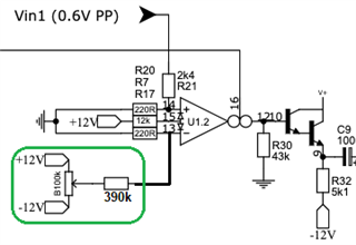
As you can see in the schematic, Iabc of each half of the LM13700 is maximum 500uA.
Vin1 and Vin2 are normally 0.6V PP but for this example, they are both 0V in order to show the issue. So no signal goes through the non-inverting inputs!
Iabc are controlled by a potentiometer and an external voltage control. 
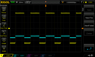
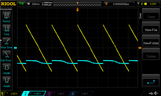
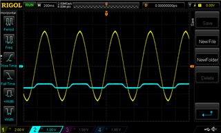
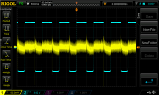
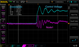
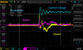
I noticed something very unpleasant when I feed a control voltage (on the left of the schematic). this is 10VPP and it also appears at the output as Captured by the oscilloscope. This is unexpected to me since if no signal is applied to the non-inverting inputs, I expect nothing at the output as well.
Do you know why this is happening and how i can avoid it?
Thanks


  • Hello Jacopo,

    This is caused by the input offset voltage ; VOS including diodes; Diode bias current (ID) = 500 μA  is 0.5mV typical and 5 mV maximum

    The input offset voltage is part of the input signal that the LM13700 amplifies. The amplifier only truly has zero input when input is -1 * Vos.  This could be done with potentiometer in similar way as the op amp on left is nulled.  Adjust new pot until output is minimized.  

  • Thanks for the help Ron, would you mind to elaborate a bit the answer?
    I'm having hard time to understand what precisely you mean and i really care to get the details.
    So you suggest to add a potentiometer that adds  -1 * Vos on each non-inverting input? or where?

  • Jacopo,

    Like this in green box on IN-. If preferred, this could be moved to IN+ side instead.

    Do the same on the other half LM13700. Two pots added because the Vos of each half of LM13700 will be different 

  •  this made it much much better and now the signal at the output is around 50mV that is more than acceptable. Thanks for the advice. 
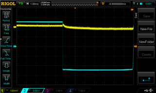
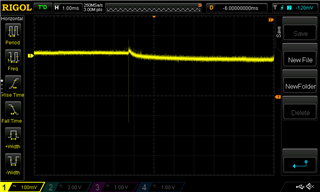
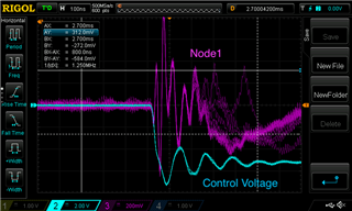
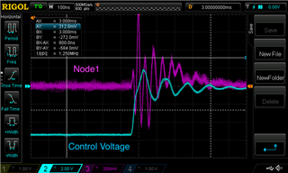
    When the control voltage goes abruptively negative though, i still get a spike of around 300mV (as you can see in the picture). 
    Can I make it even better than this somehow?

  • Jacopo,

    Edges contain very high frequencies. Higher than LM13700 can process. Same goes for the U2.2 op amps and your PNP diff amp. 

    Check the signal path. Does the glitch also show on U2.2 pins 6, 7 and LM13700 pins 1,16?

    U2.2 might not be needed at all. A passive divider could be used to scale input for the diff amp.

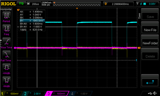
  • Not in the virtual ground but on pin 7 of U2.2 indeed the high frequency is present, but not as a glitch... the control voltage is in fact the blue square wave in the pictures above (with sharp edge).
    That's translating the signal as a current via the PNP current source and then the 2x IABC flow into pin 1 and 16.
    As you say, It looks like the LM13700 can not keep up with the sharp edge of the square wave but I was not aware to those limitations at all.
    What are they called in the datasheet?

  • Jacopo,

    If the glitch is always negative then I suspect that Q9 (NPN) is slightly faster than Q11 (PNP) transistor (see figure 16).

    Nothing specific in data sheet. However in data sheet Iabc doesn't drop below 100nA.  Adding a resistor from +12V to pin 1 that passes at least 100nA would keep the amplifier slightly on at all times. Do same for pin 16. Perhaps this would reduce the glitch. 

  • Hello again. I tried to add a resistor from +12V to both pin 1 and 16 (feeding a constant 1uA on both pins) but this didn't help.

    On the datasheet (fig.22) there is an example of Amplitude modulator and the configuration is very similar to a standard VCA configuration. I wonder how this can be tolerated since that audible glitch would be present as well.
    Nobody had that inconvenient? Strange.
    Of course the frequency of the glitch is the same as the frequency of the modulator.

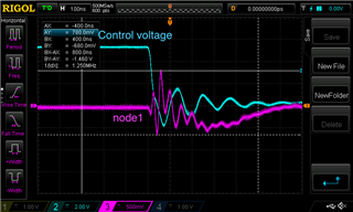
    So, it looks like this issue is not dependent from IABC being at least 100nA but the more when the edge abruptly rises and when it falls. At least this is my understanding from what i captured with the oscilloscope.

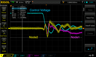
    I marked as Node1 and Node2 the points where i placed the probes of the oscilloscope.

    The picture are taken after I minimized VOS as much as possible, as you suggested.
    Also, the in blue is the control voltage.

    -when is 5V, this correspond to 500uA on pin 16(half of LM13700 with purple trace on the oscilloscope)
    -when is 0V, this correspond to 250uA on pin 16
    -when is -5V, this correspond to 1uA on pin 16
    those values are inversely proportional to pin 1 (half of LM13700 with yellow trace on the oscilloscope)


    Hope someone will be able to help me understand this!

  • Jacopo,

    Section 7 of the data sheet explains how the LM3700 operates. The output current is the sum of two equal opposing currents that change value quickly when Iabc current changes quickly. The time delay of these two currents won't be perfectly matched.

    Slowing the control signal will reduce the output transient. Adding a capacitor across R26 will slow U2.2 pin 7 slew rate so the final Iabc current slew rate will also be reduced. Experiment to find the best compromise value. Between response time and transient reduction. 

    If the glitch is always negative then I suspect that Q9 (NPN) is slightly faster than Q11 (PNP) transistor (see figure 16).