This thread has been locked.

If you have a related question, please click the "Ask a related question" button in the top right corner. The newly created question will be automatically linked to this question.

OPA4192: Settling Time circuit topology for Data sheet and Typical Characteristics

Part Number: OPA4192
Other Parts Discussed in Thread: OPA192, OPA2156, OPA828, OPA827, OPA992, OPA323, OPA4323, OPA322, INA851,

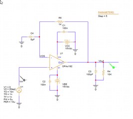
I'd like to know the circuit topology when the settling time is specified.  The Pspice model I use from the website gives me a much better settling time than the typical that is shown in the datasheet.

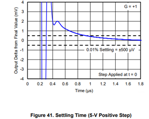
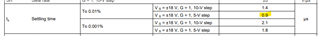
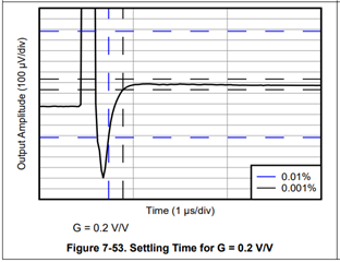
  1. Datasheet page 9 ts.  I see Rload is 10K (from the top of the page), any load capacitance?
    1. Note that the typical step responses use a Rload of 1K and Cload of 10pF.  There responses are even faster than the typical that is specified in the data specification table.

Thanks,

-John Gray

  • Hi John,

    The data sheet shows settling time plots on page 19; those are the best to reference for more detail:

    For this plot, the conditions are listed as 10 kOhm RL and 100 pF CL.  This lines up well with the data sheet spec. of 0.9 us:

    When I simulate this in TINA, I do get a bit faster response:

    I'm seeing 810 ns vs. 900 ns in the data sheet.  This leads me to believe that the settling time spec. must be with 100 pF CL.

    A similar response, in my TINA simulation, shows around 460 ns for a 10 pF CL.  The output capacitance will have some (although, I would have expected less) effect on the amplifier settling time because it changes the effective loop gain.  

    What settling time are you getting?

    Regards,
    Mike

  • Mike,

    Thank you for responding so quickly.  To answer your question, I get about 810nS for 5V (vs 900nS in datasheet) and 1.0uS (vs 1.4uS for datasheet) for 10V.  Matches closely to data sheet for the 5V but not the 10V.

    I have been trying to match the 0.001% numbers and they don't match at all.  I get 1.2uS for 10V (vs 2.1uS in the datasheet) and 1.05uS for 5V (vs 1.8uS in the datasheet).

    I'm using Pspice Orcad, I have not had to change any of the options.   I am using a buffer and loads of 10K and 100pF.  I have added 1K to the feedback and about 5 pF to the inverting input to simulate any trace capacitance.


    pictures above are for circuit and 5V step.  note that 5V step starts about 10nS after zero plus has a 1nS slew time to 5V.

    I think there might be another variation on the circuit.   Or the 0.001% is a 3rd or 4th order level of model parameters that are not covered by the model.  For me I used the datasheet number for 10V step as the baseline and then adjusted for my specific input parameters (20V step, multiple stages, and step response to 1 bit of 16 bit instead of 0.001%).  Then earlier I got an estimate of 15% to increase the typical step response to maximum step response and used that.  That overall increases my number to greater than 3.4uS.  I have an allocation of 2.8uS that I'm trying to meet.  I'm not sure how much help you can lend me with some of the restrictions of placing circuits on a public website.

    Again thanks for the reply.  you did point me to the 0.01% numbers that seem to be closer.

    -John Gray

  • Hi John,

    I've dug further into this; here's the most salient point -  the OPA192 has a modified compensation scheme that is not modeled in the PSPICE models. This scheme has several benefits, and generally is not observable for most performance traits.  But, the primary shortcoming is that settling time at very low voltages (i.e. 10's of uV) can take longer. 

    The PSPICE and TINA macro-models use our GWL model approach that is very accurate compared to older Boyle models, but this small variation on the compensation is not captured, therefore the model would tend to give slightly faster settling time results. 

    So, for your case, I would trust the data sheet, which apparently is suggesting that the OPAX192 will not work.

    Can I help recommend a faster amplifier?  OPA2156 is also CMOS, R-R input, but a much higher bandwidth and faster settling.  Or are there any key parameters that can help narrow down the search?

    Regards,
    Mike

  • Mike, thank you for getting back to me and explaining the possible reason why the model may not match the datasheet on the 0.001% settling times.  I would like to see if you can help with an op amp recommendation for the configuration.   I'll need to do this with some generalizations of the topology and not diagrams.  I thought that this might be best way in the public domain and maybe the most educational also.

    The op amp OPAx192 is used in an ADC conversion system.  specifically, it's after an 8:1 mux.  The signal range into the mux is ±10V.  Due to the input impedance into the mux we have a buffer on the output of the mux that drives a gain and level shift into one side of the ADC.  there is an inverter and level shift driving the other side of the ADC to make a differential input to the ADC.  The ADC is a 5V IC so all its signals are between 0 and 5V.  Output of the mux is ±10V, the input to the ADC is ±4.096 centered around 2.5V.  The op amp must be "mux friendly" (be able to input a step of 20V while its output is resolving from the other side of the 20V step.  The op amp must be pretty low offsets (V & I).  The buffer, level shift/gain topology must be pretty fast to settle to about 1bit (it's a 16bit ADC) in about 2.8uS.  The design has many repeats of this circuit (around 20) so the quiescent current needs to be low, we have to watch our power diet.  I think the OPA2156 will not work since it has input clamping that might affect the signal output (or would need to be buffered with resistors that might slow down the signal).  We thought the OPAx192 was the right find with low quiescent current and high bandwidth, low settling time.  When we went back to verify that the whole system settling time, we found that we were just a bit off.  So now if we can find an op amp that is just a little faster but has the same kind of offsets and quiescent current, we'd be set.

    Thank you in advance for any recommendations you might have.

    -John Gray

  • Hi John,

    Yes this sounds like the OPA192 is almost the perfect amp. for this socket.  The next step up in settling time is from OPA828; this is a new JFET-input device with very high slew rate and fast settling.  The settling time is substantially faster (110 ns settling to0.006% vs. 1 us to 0.01% on OPA192) but Vos and Vos drift is not quite as good (300 μV vs 25 μV on OPA192).  Note the 1/f noise will be much lower on OPA828 as well due to the JFET inputs(0.34 μVpp vs. 1.3 μVpp on OPA192).

    Let me know what you think of OPA828.

    Regards,
    Mike

  • Good day Mike.  The OPA828 is or at least looks like to very fast for our application.  What do you think of the OPA827, seems a little closer.  But both have quite a impact on Iq (goes from 1.0mA typ to 4.8mA or 5.5mA.  it is a big jump.  Does the OPAx992 have the same caution on the settling time (at small voltages it will be much longer)?  it seems to be about twice the speed at 0.01% settling time, has a low output impedance and only about 2.4x the iq.

    Thanks,

    -John Gray

  • Hi John,

    Yes I was thinking the Iq could be more than what you were looking for but unfortunately don't have anything that fits exactly.

    I'm not sure about the OPAx992, whether or not it has the typical compensation or the modified scheme similar to OPA192.  I'll have to loop the team that supports that device but it looks like it could work.  The only other idea I was thinking of is to use a composite amp; you can come up with more ideal settling time/Iq combinations with two separate amps.  I'll assume for now you'd like to stick with one amp, let me loop the General Purpose Amps. team for feedback on the OPAx992 settling time.

    Regards,
    Mike

  • Mike, thanks again.

    I agree that the Iq is more than we were expecting for the opa828 plus I see the saturation voltage of the opa828 is high, from 1.2 - 2V depending on what you are looking at.  this won't do well in the 5v supply position.  As an information item we want to use 5v supplies on the last stage going into the ADC to make sure the opamp doesn't go over the 5V supply on the ADC (we have found some converters have issues with that).  The op amp out of the mux would have a power supply of 15V and the opamp feeding the ADC will have a 5V supply (the same as the ADC).   If I failed to mention that I apologize.  

    That sounds like it leads to a composite opamp selection for the configuration.  So go ahead and suggest a couple of sets and see what happens.

    Thanks,

    -John Gray

  • Hey John, 

    Output of the mux is ±10V, the input to the ADC is ±4.096 centered around 2.5V.
    As an information item we want to use 5v supplies on the last stage going into the ADC to make sure the opamp doesn't go over the 5V supply on the ADC (we have found some converters have issues with that).  The op amp out of the mux would have a power supply of 15V and the opamp feeding the ADC will have a 5V supply (the same as the ADC). 

    These numbers are not making a lot of sense to me, please confirm if I am misunderstanding. 

    OPAMP1 from MUX OPAMP2 to ADC
    Power Supply 15V 5V
    Input 20V (±10V)
    Output 8V (±4V)
    Target Iq
    Target Settling Time 0.001%  2.8us

    All the best,
    Caro 

  • Caro, sorry for any confusion.   

    Signal out of the Mux is ±10V.  Supply on op amp from mux is ±15V.  Configuration currently is a non-inverting buffer.

    Signal out of the Buffer (from above) is ±10V goes into a gain and level shift configuration that outputs 0 to 5 volts centered around 2.5V.  Supply on this gain and level shift is +5V.  

    Signal out of the gain and level shift configuration drives into the ADC +in and drives an inverter opamp that outputs to the ADC -in.  This inverter and level shift that outputs 5 to 0 centered around 2.5V and it is also powered by a +5V.

    I hope that helps.

    -John

  • Hey John, 

    Understood, in that case I recommend OPA992 be used for the first one and OPA323 be used for the second one.
    I think we currently have only released the OPA4323 but the single channel is likely to release in the next couple of months. 
    If the project timeline is tighter, we historically have recommended the OPA322 for ADC applications. 

    The OPA992 has a different compensation scheme than the OPA192. 

    Unsure how far along the design is but if needed, please leverage this FAQ for the voltage scaling aspect: [FAQ] Voltage scaling for almost any application (single ended)

    All the best,
    Caro

  • The OPA992 sort of fits my application, but using a brand-new part that is only available in a quad might be an issue for us (OPAx323).  I'll have to evaluate it a little more.  Of course, using the OPA992 does work nearly except for the Iq and Vos.  We need to evaluate it a little more.  

    I wonder if a single ended to differential output would be a better fit?  Needs a gain of 0.4V/V and again going from a ±10.24V max signal range to about ±4.096V range centered around 2.5V differential.  Is there an area of components that might work for ADC conversion?

    Note to readers.  Question copied from OPA140: input common-mode voltage specification - Amplifiers forum - Amplifiers - TI E2E support forums to keep like discussions together.

    Thanks again everyone.

    -John Gray

  • Hi John,

    Thanks for bringing your question back to the original thread.

    I am considering our single-ended to differential options, and I believe we should be able to find a solution that meets your specific requirements. Will provide an update tomorrow.

    Regards,

    Zach

  • Hi John,

    The best INA options with differential output are the INA851 and the PGA855 as these have excellent settling time, See figure 7-53 for INA851.


    Of course the faster settling time comes with higher Iq, there is really no way to avoid this. I see you mentioned previously that you require fast settling and low Iq but you did not provide an exact power budget. Do you have a max Iq spec you need to meet for this amplifier stage?

    Due to the input impedance into the mux we have a buffer on the output of the mux that drives a gain and level shift into one side of the ADC.  there is an inverter and level shift driving the other side of the ADC to make a differential input to the ADC.

    Can you provide a schematic for your circuit? I believe you are describing something like this: Single-ended to differential using a two op-amp circuit

    Thanks,

    Zach

  • Zach, Good day and hope all is well.   I agree with you that INA851 looks very good.  Yes, the Iq might be a bit big.  But I think big issue would now be the package.  A leadless package is not allowed, sorry.   The budget is really power for us.  So, I think the selection would be to get close to 1 uS settling time and similar Iq as the OPA4192 (I know that is a dream).  So, then I would ask for the lowest Iq with a settling time of about 1 uSec.   And I do like the instrumentation amps with differential outputs built for ADCs.  That would allow for us to remove the buffer after the Mux and integrate the discrete differential drive that we have.   let me add the "circuit" here when I can draw it without information that shouldn't go out to the public.

    And we are not opposed to using other op amps to create the function of ±10V input to 0 to 5 voltage output to drive the ADC.  I'm starting to think to a "composite" solution that would be a fast op amp at the output of the Mux and a more power savings op amp in the conversion of level shift and gain (well really attenuation).  Let me work on the "schematic".

  • Hi John,

    That is too bad that the leadless package is disallowed for this design. Otherwise, I think the INA851 would be perfect if you can budget the additional Iq, 7mA (max @25C) vs 4.8mA (max @25C) for OPA4192.

    So, then I would ask for the lowest Iq with a settling time of about 1 uSec.

    If Iq is of utmost importance, it seems that the design tradeoff may be to continue with your original OPA4192 design as this put you very close to your 1μs settling time with minimal Iq.

    I agree that a composite solution can be achieved, but this will require additional op amps that must have higher IQ than the OPAx192 to achieve the faster settling time as discussed above. Going down the composite route will likely end up with higher overall Iq than the single IC INA851 solution.

    It would be best if you could provide a detailed schematic showing the entire AC signal chain. Block diagrams or overly simplified schematics may exclude important details that are critical to our analysis and design recommendations. I understand your concerns with posting the detailed schematic on the public forum. If you prefer, you can send me the schematic over private message.

    I sent you a friend request on E2E, this will allow us to communicate off of the public forum.

    Regards,

    Zach