This thread has been locked.

If you have a related question, please click the "Ask a related question" button in the top right corner. The newly created question will be automatically linked to this question.

LMH34400: What is difference for LMH34400 output when enable / Disable Ambient Light Cancellation Mode ?

Part Number: LMH34400
Other Parts Discussed in Thread: LMH6611,

Hi TI,

What is difference for LMH34400 and LMH6611 output voltage when enable / disbale Ambient Light Cancellation Mode of LMH34400?

According to LMH34400 data sheet :

7.3.3 Single-Ended Output Stage
The output stage of the LMH34400 has a 10-Ω series resistor on its output to isolate the amplifier output stage
transistors from the package bond-wire inductance and printed circuit board (PCB) capacitance. The net gain of
the LMH34400 (TIA + output stage) is 40 kΩ when driving an external 100-Ω resistor. When the external load
resistor is increased above 100 Ω, the effective gain from the IN pin to the output pin increases. Consequently,
when the external load resistor is decreased to less than 100 Ω, the effective gain from the IN pin to the output
pin decreases as a result of the larger voltage drop across the internal 10-Ω resistor. When there is no load
resistor connected to the output pin, the effective TIA gain is 44 kΩ. The output voltage of the LMH34400 is set
to a fixed value of 1.0 V when there is no current flowing into the amplifier. The output swings above and below
1.0 V when the photodiode sinks and sources current, respectively.

For below schematic, if there is no input ,whether is LMH6611 output voltage expected @3.5V (1V x 3.5 (LMH6611 gain)) ?, but actually to measure LMH6611 output volatge is 3.29V , why?

if input 19.5uW into PD-3 and expected 18.5uA flow into LMH34400, whether is the LMH6611 output DC level @3.5V (1V x 3.5) ? and the LMH6611 output swings above and below 3.5V ?

and is the swing volatge level @ 18.5uA x 40 K x 3.5 = 2.59V which is over the supply volatge @4.5V (+Vop)?

For below schematic, how to connect  external 100-Ω resistor for LMH34400's loading ?
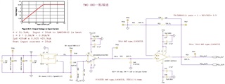
  • Hi Jerry,

    The LMH34400's DC cancellation loop is used to cancel any voltage offsets resulting from ambient light. This will effectively remove any DC offset seen at the output of the LMH34400 caused by ambient light. Disabling this feature could result in an offset being measured at the LMH6611 output. There could be a few reasons for the discrepancy between the 3.5V expected signal and the actual 3.29V you are seeing. One could be that there might still be a tiny amount of current being amplified by the device which results in a slightly lower value than the ideal 1V at the output. The datasheet also highlights that the default output voltage can range from 0.93V all the way to 1.07V. Could you probe at the output of the LMH34400? If this is under 1V in combination with resistor tolerance, this could the reason for the 3.29V at the output of the LMH6611. 

    As for the question regarding the output voltage of the device, the LMH34400 will default to 1V and swing below the 1V if the photodiode cathode is biased to a positive voltage (device is sinking current) and swing above 1V if the photodiode anode is biased to a negative voltage (device is sourcing current). When sourcing current the total output voltage will be the sourced current * LMH34400 V/V gain + 1V LMH34400 default output offset. With this information, 18.5uA would result in an output voltage around 1.8V. This value gained by 3.5V/V in the LMH6611 gain stage, will result in an output voltage range violation due to supplies of the LMH6611 being +4.5V. 

    Best Regards,

    Ignacio

  • Hi Ignacio,

    Thanks for your quickly feedback my questions about LMH34400

    18.5uA would result in an output voltage around 1.8V – why is it around 1.8V ?,

    would 18.5uA result in an output voltage @1.74V (1.85uA x 40K + 1V)?

    Original thinking for this circuit, I would like that LMH34400 + LMH6611 amplify the photo diode 's current 18.5uA to around 3.5V, it means that I should put AC couple capacitor (1uF) between R25 and pin3 of LMH6611 to remove 1V DC offset and set LMH6611 gain arond 4.8V/V to achieve output volatge around 3.5xV ?

  • Hi Jerry,

    The reason I said it would be closer to 1.8V is because the gain of the TIA from the input to the output is around 44k as the output is going into a high impedance node. The 40k gain is under the assumption that the LMH34400 is driving a 100-ohm load, as this load creates a voltage divider with the 10-ohm internal series resistor. Section 7.3.3 Single-Ended Output Stage highlights this in more depth.

    You should be able to reconfigure the circuit to remove the 1V DC output offset and adjust the gain accordingly like you suggested. I attached a circuit from TINA that can be a good starting point for your design. The actual circuit will likely require some tuning as the model does not exactly model non-idealities of the devices and components but modeling the circuit is a good starting point. 

    Best Regards,

    Ignacio

    LMH34400+LMH6611.TSC