This thread has been locked.

If you have a related question, please click the "Ask a related question" button in the top right corner. The newly created question will be automatically linked to this question.

OPA2156: Expected operating temps under bias

Part Number: OPA2156
Other Parts Discussed in Thread: TINA-TI

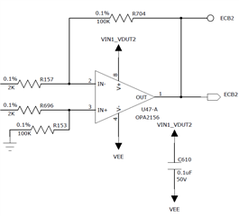
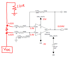
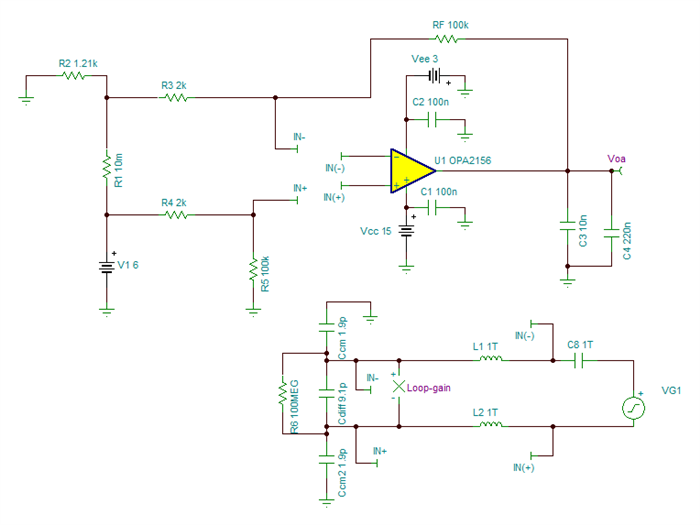
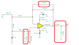
I'm using the OPA2156 for a very simple circuit measuring drop across a .01 Ohm shunt resistor.    My circuit operation seems to perform as expected but I was surprised by the temperatures I was reading on the IC when using a thermal camera.   The positive rail is biased with a 15V supply and the Negative (VEE) is -3V.     There is a dual op-amp package although I'm only using one of the channels.    My test conditions are running board at 25C ambient, the shunt resistor is not loaded so there is 0V drop.   When there is no voltage applied to the shunt resistor my IC is sitting around 40C which seemed reasonable to me given the Pd and thetaJA of 119degC/W.    If I apply 1V to the shunt resistor the IC temps jump to 70C,  if then increase the shunt resistor voltage source to 6V the IC then jumps to 90C.     The output of the op-amp is driving the input of an A2D converter although in my examples above the voltage on the output stays below 50mV as there is no load on the shunt.    

I don't see how changing the shunt resistor voltage while not driving a load on the output is causing such high increases on my IC temps.    I was thinking it would take almost 400mW of additional power to raise from 40-90C.    Is there something I'm missing with how my voltage inputs are impacting power dissipation?

  • Hi Douglas,

    I need to ask a couple of questions to help debug the issue.

    Can you please clarify, what is the common-mode voltage of the 0.01Ω of the shunt resistor with respect to the OPA2156 local ground?  In other words, is this a high-side current sense resistor sitting at a high-common-mode voltage? or is the shunt resistor referred to the same local GND of the OPA2156?  When you apply a 1V voltage to the shunt, does this mean a common-mode voltage to the shunt referred to the same ground of the OPA2156? 

    Please draw in the schematic/diagram above the shunt resistor connections, showing both the common-mode voltage supply with respect to the OPA2156 local ground, and the differential voltage across the shunt to ensure we understand the test conditions.

    You have explained that the OPA2156 difference amplifier circuit is driving an ADC (A2D).  Is there an RC filter between the A2D and the OPA2156?  If yes, what are the R C values? 

    How many boards or devices show this issue?  Is this an engineering prototype, soldered by hand or a board that went through a standard solder re-flow and clean process?

    Thank you and Best regards,

    Luis


  • Hi Luis,  Thanks for the quick reply.    I've updated the schematic image to illustrate the setup that I was measuring under.   This is a high side sense resistor with Vdc being programmable (1V and 6V during my tests) and then just a fixed 1.21K resistor on the other side of the shunt.   The application will have a different load source but right now to simply this issue I'm focusing on the no load condition. I've also added in the voltages I've measured at different nodes.

    The output of the op-amp is not driving an RC filter but does have a .01uF and .22uF cap to GND local to the A2D input.  These are prototypes and same behavior is seen on both of them.  Boards went through the standard process of solder and reflow.

    Thanks,

    Doug

  • Hi Douglas,

    The OPA2156 will not be stable driving directly the relative large capacitance of .01uF and .22uF cap to GND at the ADC input.  Can you please check the output with an oscilloscope when the issue occurs for oscillations?

    An open-loop small-signal stability analysis in TINA-TI using the OPA2156 model shows that the circuit is un-stable with an abrupt change in phase while driving the relative large capacitance.  Please see simulation below.  The difference amplifier circuit will need to use an isolation (compensation) resistor between the output of the op-amp and the capacitor at the ADC input to stabilize the circuit, and we would need to select the resistor and capacitor value depending the ADC sampling rate and sample-and-hold settling requirements.  

    What ADC device are you driving, is this a SAR or Delta-Sigma? and/or what is the sampling rate (or acquisition time)?

    Or what is the resolution of the ADC, and sample-and-hold cap value and full-scale voltage? 

    Thank you and Best Regards,

    Luis

  • Hi Luis,

    You are correct, I do start getting oscillations when my supply is turned on at both 1V and 6V.     I’ve added some plots below as well as our max voltage condition of 12V below.  I am using a SAR A2D that is integrated in with our uController.    This is 12bit with 5V reference.  The sampling rate is 17us.

    1V Condition:

    • 1.7V p-p centered around 0V
    • 68.5KHz Oscillation
    • 71C

    6V Condition:

    • 836mV p-p centered around 0V
    • 270KHz oscillation
    • 90C

    12V Condition: 

    • 956mV p-p centered around 0V
    • 286KHz Oscillations
    • 93C

    Thanks,

    Doug

  • Hi Doug, 

    I do start getting oscillations when my supply is turned on at both 1V and 6V.

    You would need to compensate the feedback loop and remove the loop instability from the difference amplifier.

    we would need to select the resistor and capacitor value depending the ADC sampling rate and sample-and-hold settling requirements.  

    I tried to compensate the op amp, but it has to lower the BW of the op amp, but the circuit needs to have higher BW at a rate of the 17usec. You may have to lower your capacitive load (230nF) or increase the Rsense and lower the gains. 

    If you need to further assistant, please let us know. 

    Best,

    Raymond

  • Hi Doug,

    Since you are driving an ADC, using relatively slow sampling rates (17us), an RC filter with Riso=~499Ω and C=550pF should work well with the ADC, while the difference amplifier remains stable.  Adding a 10pF capacitor on the feedback, and a 10pF in parallel with R153 improves phase margin further.

    Below is the stability analysis of the proposed circuit above:

    Thank you and Best Regards,

    Luis Chioye