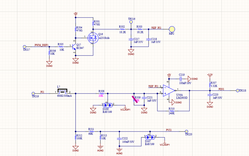
1. The file is a record of the customer's test. 2. The output frequency of the customer application is abnormal with the standard test frequency, the schematic diagram is as shown below, it is a channel of frequency input, PI1 is the frequency input of the product, and it enters the + input terminal of U56A of LM2903 through embedding and filtering; -The input terminal is to adjust the voltage of the threshold, PWM adjustment is carried out by the PWM_REF1 pin of the MCU, the output REF_PI1, the signal adjusts the output range of 0~5V, connected to the -input terminal of U56A, after the comparison of U56A, the output signal PIN1 is connected to the pin of the timing frequency of the MCU.

-
Ask a related question
What is a related question?A related question is a question created from another question. When the related question is created, it will be automatically linked to the original question.