Because of the holidays, TI E2E™ design support forum responses will be delayed from Dec. 25 through Jan. 2. Thank you for your patience.

This thread has been locked.

If you have a related question, please click the "Ask a related question" button in the top right corner. The newly created question will be automatically linked to this question.

OPA2191: Max Load No Snubber Circuit

Part Number: OPA2191
Other Parts Discussed in Thread: TINA-TI

Hi Amps Team,

We are working to optimize the PCB by reducing the number of components in the schematic. One possible way to reduce components would be to remove the snubber circuit. Please note that the datasheet for the OPA2191 component recommends placing an RC circuit with unity-gain configurations that have no/light DC loads. Would you please advise what would be the maximum load that we could have without said snubber circuit? Thank you for your help.

Best regards,
Nic Gough

  • Hi Nic,

    Let me start by clarifying what is meant by load in this context.

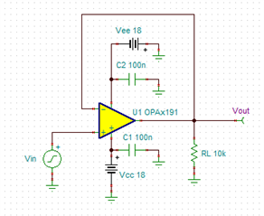
    Typically a high load indicates a high output current from the device, in this case the load is considered with respect to the amplifier's output stage. This is easily confused with the load resistance often referred to as RL, which is present at the output of the amplifier. See schematic below.

    There is an inverse relationship between the load resistance (RL) and the current load on the amplifier's output stage. For high values of RL there is very little current that the amplifier's output stage needs to provide, and this is a light load. For low values of RL, the amplifier must provide much higher output current for the same output voltage, and this is considered a heavier load on the amplifier.

    Therefore, the maximum load is the short-circuit current limit of the amplifier. As the datasheet describes, the snubber circuit is only required for no/light DC loads. I believe the question is what is the minimum load that can be achieved without the snubber circuit.

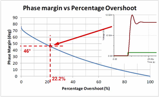
    The purpose of the snubber circuit is to stabilize the amplifier in light loading conditions. Therefore, the minimum load that can be achieved is the load that results in acceptable phase margin and transient response. Typically, a phase margin >45° is considered stable, although certain applications may require up to 60° of phase margin.

    You can measure the phase margin indirectly based on the % overshoot at the amplifier's output in response to a small-signal input voltage step.

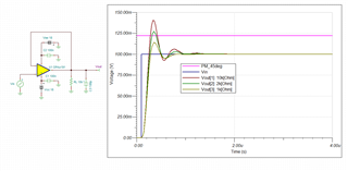
    I simulated this in TINA-TI for a load capacitance of 100pF and sweeping the load resistance at 10kΩ, 2kΩ, and 1kΩ. The pink line represents 22% overshoot which corresponds to approximately 45° of phase margin. In this case, the amplifier has less than 22% phase margin for a resistive load of 1kΩ.

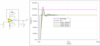
    The stability is highly dependent on the capacitive load on the output of the amplifier. Simulating again for a load capacitance of 50pF shows that the amplifier has less than 22% overshoot for resistive loads of both 1kΩ and 2kΩ.

    I've attached the TINA simulation file below. Feel free to adjust the simulation to meet the exact output conditions of your circuit to determine your minimum stability criteria.

    OPAx191_Load_Sweep.TSC

    Regards,

    Zach