This thread has been locked.

If you have a related question, please click the "Ask a related question" button in the top right corner. The newly created question will be automatically linked to this question.

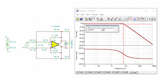
THS4561: Bode mismatch in TINA

Part Number: THS4561

Accordins with the equations in the chapter 7 of this doc :Active Low-Pass Filter Design (Rev. D) I dont get the same Bode graph using this values in TINA (attached).

Where is the error in my TINA design? I can adapt my bode but I lost the Q value so I lost the Butterworth condition....

I need a LowPass ButterWorth 2nd order fc=7200Hz

2ndBWlow7k2.TSC

  • Hi Alberto,

    I have reviewed the TINA schematic that you have attached. I believe that the error in your TINA design, is due to the placement of C3, R2, and R1. Due to the placement of these components, the amplifier is no longer operating in a MFB topology like you are trying to achieve from chapter 7 of the reference document.

    I have adjusted the layout as shown below, and now the device is achieving the desired filter characteristics. I have also attached the TINA schematic I used below.

    THS4561_MFBLPF_E2E.TSC

    Please let me know if you have any other questions.

    Thanks,

    Nick

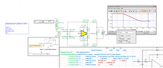
  • Hey Alberto, here is your design adjusted for a lower noise implementation. I always look out to 200MHz on this part for resonance, yes - there it is at 95MHz. Moving the feedback caps outside those 20ohms inside the loop helps this, you might try increasing those a bit also. I did not run a phase margin test, maybe Nick can do that  - this resonance is coming from the open loop output impedance resonance. 

    7200Hz 2nd order MFB LP.TSC

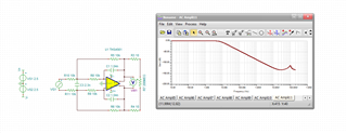
    And here is Nick's design run out to 200MHz, yes, a little sharper resonance, 

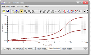
  • And, as long as I have both files open, here is the comparison of output integrated noise, the lower curve is the improved RC values - this design might could use a post RC filter in the 100kHz region to bandlimit the total RMS output noise, 

  • Thank you very much to both of you!!

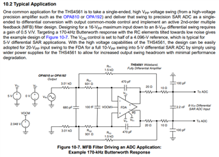
    The PCB is already manufactured so I can`t add new components. I based the designe in this schematic of the THS4561 datasheet:

    The 20ohms resistor proposed to decrease the noise could be placed in this other position?

    I forgot to include a voltage follower after the voltage divisor so I am having troubles applying the Q and Fc equations (I attach the schematic).

    Do you know how to calculate the particular equations of my weird topology?

    I want to use 1% tolerance capacitors and 0.1% resistor capacitors. Does Tina or FilterPro have a tool to minimize the error made normalizing the passive values?


    2727.THS4561_MFBLPF_E2E.TSC

  • You have everything there, that 1fF in Fig 10.7 is just a parasitic placeholder. the feedback cap would be better on the other side of the 20ohm and you should tell us you post RC values. So you should be ok just changing values. I don't think any of the TI tools trys to minimize fit error snapping to standard values. I typically suggest 0.5% R's in E96 values and 2% C's in E24 values. 

  • What do you mean with 1fF? My RC values in the output are 200MHz & 20pF (ADS131E08IPAGR)

  • the Figure 10.7 you pasted in had 0.1pF across the inputs, ignore that. I don't know what you mean for RC values, look at figure 10.7 you said you were following and the RC values after the output of the FDA, do you have those and what are they

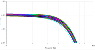
    Here is a 200case Monte carlo with Guassian Rs at 0.5% and C's at 2%