This thread has been locked.

If you have a related question, please click the "Ask a related question" button in the top right corner. The newly created question will be automatically linked to this question.

INA215: Pics glitch when input commutation on INA21x

Part Number: INA215
Other Parts Discussed in Thread: LM393, INA240, INA212,

Hello

I am using 3 current-shunt AOP with NMOS transistor switching from1 one to an other (goal is to measure current on a wide range of current from µA to A so we switching from 3 INA with different shunt/gain)

I see some glitch or pics on INA ouput when NMOS commute, do i have to add extra filtering on output to avoid these pics ? or modify input commutation ?

mes_sleep is connected to LM393 comparator and a ADG704 mux

  • Hi,

    I’m guessing the load is connected to “MOT_RSS_OUT”?

    Adding some gate capacitance to Q1 will slow down the turn on/off rate, which may help reduce peaking. Output filtering is typically not effective in this situation.      

    A better solution is to move the current sense resistor to either of two locations – (1) between “MOT_RSS_IN” and Q1, or (2) between the load and GND. This change should avoid the output peaking in the first place.

    You could also choose INA240 or INA241 for this application. These devices fit better for the use case.

    Regards, Guang

  • Hi

    Sorry for late reply, so you recommend to use a high side measurement instead of low side ?

    mes_sleep is splited to LM393D comparator and ADG704 mux and it seems i have some problem... There is a adaptation from signal output of INA212 to ADG704/AG393 to do ?

    Why are you recommend the INA240/241 instead of INA212 maybe you think we use PWM on our MOSFET but basically we don't switch command on MOSFET just "mode" : standby, sleep, normal and we choose INA212 for the high gain and measure µA.

    Regards

    Kévin

  • Hi Kevin,

    It was not clear from the schematic what sensing topology is being used. It is good to know that low-side is the chosen one. In that case, there is no need to switch to a different amplifier.

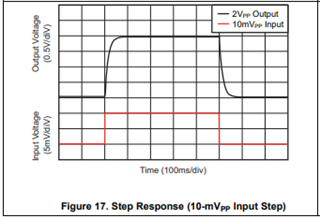
    You can certainly try output filtering. I still wonder if there are other factors though. Because the typical step response should be fairly flat as shown in this curve:

    Regards, Guang

  • Thanks, yes maybe schematic is not clear, current measure is mes_sleep and splited into 2 going to an AD704 mux and LM393 comparator.

    I have try to isolate each part on my board and it seems that the issue on INA212

    I have check +12V iso of the photocoupler : ok

    I have decrease the value R10 and R11 on schematic R10=270ohm and R11=100

    I also add a capacitor of 100nF in parallel of the shunt resistor

    Nothing solve my problem yet i always have a pics on INA212 output corresponding to INA212 supply (around 3.3V) during more or less 200µs after voltage decrease to nominal value measure from the INA212 sensor. 

    I don't know what to think... It can be an issue of supply decoupling ? ground of signal measure is to the same that INA212 ground, do i need to add extra filtering ? check VGS signal..

    Every advice is good to hear :)

  • Hi Kevin,

    The plateau lasts too long (~300uS?) to be attributable to transient response alone. It looks as if the inputs are being held to cause the output to rail. 

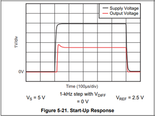
    Is channel one the power supply? Your setup is similar to below “start-up response”, although REF pin is grounded in yours. I expect similar response despite the minor setup differences:    

    Since you do have some on/off operation at the input, it is a good idea to inspect the input voltages as well.

    Regards, Guang

  • Hi Guang,

    Thanks again for your support, i have try different test:

    Adding decoupling on TLP152

    Modify R11 résistor (try with1k, 2.7k)

    Adding resistor between gate and source, also a 100nF cap

    I also check +12 iso, +3.3V and power supply (MOT_RSS_IN MOT_RSS_OUT), i see no variation on voltage during transition, with power supply turn off problem still exist

    I always see this front at +3.3V during around 300µs on INA212 output, 

    Is it a schematic issue with different ground ? wrong value ? from my point of view it's MOSFET commutation that disturb the measure...but i don't how to solve it Slight smile

    Edit : with an others sensor INA215 and Shunt=0.33ohm it seems i don't have the problem, i try to measure very low current with high gain system and that the root cause i think (33ohm and INA212 (g=1000) also try with 470ohm and INA215(g=75) same result)

  • Hi Kevin,

    If you have two different grounds, I would connect them for now just to eliminate a variable.

    What kind of load is connected? If there is a large capacitive load, I would replace it with a resistive load for experiment. Another thing to try is to decrease Rs1 to much smaller values, such as by 10x (potentially all the way to 0, ie, shorting the input).

    Another, more involved, experiment is to replace the MOS switch with something else such as a relay.

    I would start with the easier ones and implement one at a time. I’m hopeful that you'll see a change in behavior somewhere along the way.   

    Regards, Guang

  • Experiment a way to filter the 200-300µs at output of the INA215 is possible you think ? or with inductance before the shunt ?

    With the current range i have,  i can't change shunt/INA values ... maybe there a better way to measure µA with INA215

  • Hi Kevin,

    The proposed experiments involve temporary changes. I'm not suggesting to change your design. For example, reducing the shunt value will tell us if there is any inrush current. I personally don’t think it is feasible to filter the output given the nature of the peaking.      

    Regards, Guang

  • Yes you're are right maybe i was not clear but i have an others design in parallel with lower shunt value (the test you suggest) and i have no issue, so i think the problem is to try to measure very low current with a high gain system (shunt+INA) :design seems working

    So i have to try to find a way to "filter" the pics that is amplified, at the input or output of the INA215 

  • Hi Kevin,

    Sounds good.

    Given your good experience with the other similar design, I think you’ll be able to figure out the root cause. It is fairly clear now.

    If you care to share your solution, please post back in the future.     

    Regards, Guang

  • Hi, I think the problem is solve adding a RC filter a the output (220ohm and 330nF during my test) pics voltage is filtered and the rest of my schematic is not affect, thank again for your help and support

  • New "issue" :) i have a shunt of 3mohm on a INA215 (to measure big current value), i use a dynamic load for current load. For exemple when i set 0.2A on my load, i expect to measure with INA215 0.003x0.2x75=45mV on the output (power supply deliver 0.2A) ? but i measure 160mV, i can consider difference with tolerance of the shunt 1% or Rds On of the MOSFET but it's huge no ? maybe i miss something ?

  • Hi Kevin,

    I suppose this is DC test.

    That indeed is a large deviation, even considering INA215 offset etc. Although not a root cause for what we’re concerned with here, swing is something we need to pay attention to when testing with small current (or small shunt voltage).

    Can you steadily increase the current by steps, and measure the input differential voltage as close as possible to the INA215 IN+ and IN- pins, in addition to the output voltage.

    Once the data is tabulated, hopefully some pattern will emerge.

    Regards, Guang

  • Hello Guang,

    I made some measurement with different value of power with my dynamic load (from 0A to 0.8A) linearity is good and amplification stage seems ok.

    I "just" have a strong difference and i suppose i have an issue on my PCB because i have a 3mohm resistance and think with my lab measure and maybe not a perfect routing on PCB, these increase the shunt value and give those values..

    I think to increase the shunt resistance and decrease the gain with a different INAXX what do you think ? to have less impact with my PCB but i have to choose good shunt to allow high current around 40A

    Edit : what do you thing of INA240 use with 5mOhm 10W shunt ? it allow me to measure over 30A, INA240seems to be close to INA215 with PWM rejection added at the input

  • Hi Kevin,

    You’re correct that a larger shunt resistor will suppress more those unwanted parasitic effects due to layout and manufacturing (such as soldering). So yes, if you can use a larger resistor, definitely go with it.

    INA240 is a new generation amplifier with high precision. I think you’ll see improvement with it in terms of total output error.

    Regards, Guang

  • Thanks  i will try the INA240 with higher shunt and take care when routing pcb, thanks again for support