This thread has been locked.

If you have a related question, please click the "Ask a related question" button in the top right corner. The newly created question will be automatically linked to this question.

INA350: Output range for 0.5 Volts at reference pin

Part Number: INA350
Other Parts Discussed in Thread: TINA-TI, INA351, TMP235, TPS7A20, LM4040

Hi,

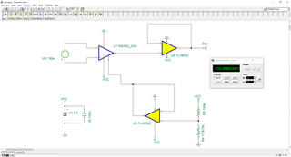
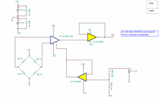
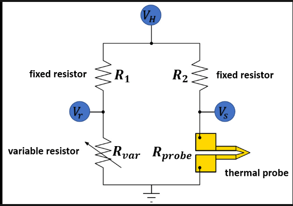
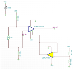
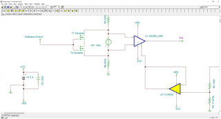
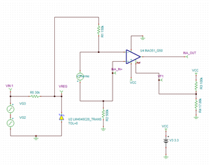
I am trying to build a circuit that amplifies the voltage for an input voltage range of -5 to 50mV. Using INA350 with a gain of 50 and the reference is set to 0.5V, further, the circuit schematics can be seen in the picture below.

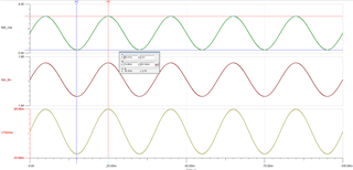
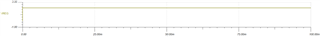
With this setup laid out in Tina-TI, I tried inputting a range of values in the voltage source VS1(-6 to 50mV) but the output stayed the same at 510mV. There may be some problem with the circuit setup I can't figure out or perhaps I am missing a crucial specification of the part(INA350). Appreciate the help.

  • Hello,

    This issue is caused by the fact that your common mode voltage is very low ~0V.

    If you try the same circuit with a resistor bridge, the circuit works perfectly fine. 

    When we look at the INA350 common mode vs output voltage plot, we see why this is the case: 

    The easiest ways to solve this problem: 

    Ensure this 30mV differential sensed voltage has some common mode element to the voltage. 

    Or, use a split supply rail to ensure the amplifier is operating in a linear region.

    Where is this 30mV Vid coming from? 

    Please let me know if you have any questions.

    Best,

    Jacob

  • Hello, 

    Additional to Jacob's response, I recommend utilizing the analog engineer's calculator that shows you how the output is affected by the common mode: 

    Here is the tool link: https://www.ti.com/tool/ANALOG-ENGINEER-CALC

    All the best,
    Carolina 

  • Hi Jacob,

    The input voltage is coming from a thermocouple. Do you have any suggestion on how to add a common mode element to the differential voltage from thermocouple. I was going for INA350 because of its price but I am also open to suggestion on using any other part.

    Regards,

    Khan

  • Hi Caro,

    Thank you for the recommendation. I was wondering what IC/part would you suggest to interface a thermocouple with a microcontroller running at 3.3V?

    Regards,

    Khan

  • Hi Khan,

    You can certainly use the INA350 for this type of application. What type of thermocouple are you trying to use?

    This is one of the more common methods of interfacing temperature sensors with an INA:

    The idea is that you form a resistor bridge, and the thermocouple temperature sets the difference in voltage between Vr and Vs. The bridge also biases the output of the bridge to have a mid-supply common mode voltage.

    If you can share the thermocouple part number, we can pick the bridge resistance and calculate the output equation for interpreting temperature.

    Thanks,

    Jacob 

  • Hi Jacob,

    I don't have a part number but I know it is a type-K thermocouple which outputs a voltage range of approximately -6mV to +55mV. Could you help with this piece of information.

    Also, I was wondering if we really need that variable resistor in that circuit? can we replace it with a fixed one?

    Regards,

    Khan

  • Hello Khan,

    Correct, that resistor could be fixed. 

    I realize since the thermocouple is operating based on the Seeback effect, we could bias the common mode with a basic resistor divider.

    Here is an Application Note discussing methods on interfacing with Therocouples: A Basic Guide to Thermocouple Measurements

    We can simply place resistors on both sides of the thermocouple to bias the common mode voltage of the INA to mid-supply. 

    I ran a simulation to verify operation, and you can see how the addition of the biasing resistors makes the circuit operate as intended: 

    INA Output (Green), Thermistor voltage from -5mV to 50mV (Yellow), INA IN+ (Red)


    I used 500kOhm resistors to form my biasing network, but you can alter these if you need to further reduce current consumption. 

    You can also consider using the INA351 if you want to remove the TLV900x buffer driver as the INA351 integrates this buffer internal to the device.

    Khan_INA_Sim.TSC

    Please let me know if you have any questions on the implementation of this circuit. 

    Best,

    Jacob

  • Hi Jacob,

    Thanks for running this simulation, the results look good.

    What precision do you think we get out of this circuit? I guess if we bias the inputs from the LDO then it may transfer errors due to its poor accuracy, right?

    Also, I was a little concerned about the offset and gain errors which would again impact the output's precision. I watched this TI's promotional presentation where the speaker provided a few techniques to deal with the errors or calibrate the circuit. I tried technique number 3 on the circuit you provided what I found was the positive range of the input works as expected but the negative input range shrinks. We can also go for technique number 1 but I don't know what kind of switch needs to go in between input pins of INA to short them and how often we need to calibrate.

    My goal is to achieve at least 12 bits of resolution, it would be great if comment on how to achieve this resolution.

    Regards,

    Khan

    Link to the presentation: www.youtube.com/watch

  • Hello Khan,

    Calibration method can depend heavily on hardware selection. 

    We have realized successful designs with both options, but option 3 typically has the capability to realize more accurate data output. 

    The INA35x has great gain error for the cost, but the offset drift sometime leads to error. What is the expected temperature range you intend to use with the temperature probe? Will the device be subjected to these temperatures as well? 

    This information will help me understand the temperature range/input voltage range for the part.

    The calibration method 1 does not necessarily have a fixed frequency for calibration routines. This frequency is typically determined at a system level with considerations for total signal chain error, and ADC sampling frequency.

    Do you know the sample rate of your ADC?

    Thanks,

    Jacob

  • Hi Jacob,

    When you said "The INA35x has great gain error for the cost, but the offset drift sometime leads to error" do you mean the gain error may sometimes be greater than the offset(1.2mV) error?

    The probe(thermocouple) is expected to be in a temperature range of -200C to +1300C, however, the device(INA350 other electronics on the board) may sit in an extreme ambient temperature range of -40C to +85C.

    The ADC has 12 bits of resolution and can sample 400KSPS which works perfectly for our application. I am hoping to get 13/14 bits of resolution by oversampling or at least get 12 effective bits(ENOB) which is our goal to get out of this system.

    Regards,

    Khan

  • The gain error is relative to the internal matching of the resistors inside the device. The offset drift refers to how the device offset voltage changes with respect to temperature. 

    The inherent offset voltage of the part will be removed through the calibration routine, leaving the primary error sources being the gain error, and the offset voltage drift. 

    Thank you for the additional information on your system, this helps us understand the measurement requirements for your system. 

    Let me run some simulations on my side to see what it will take to realize 12-bit accuracy.

    Thanks,

    Jacob

  • Thanks for the quick response. I will be waiting for the simulations.

    Also, I intend to use this on the board temperature sensor for cold junction compensation. The idea is to interface this sensor with the microcontroller and let the software take care of the compensation. Let me know what you think about this.

    Regards,

    Khan

  • Here is the part number of the temperature sensor TMP235.

    Regards,

    Khan

  • Perfect, Thanks for the part number.

    I will reply to this post when I finish the simulation profile.

    Best,

    Jacob

  • Hi Khan,

    Sorry for the delay.

    I have thought through the problem a bit more, and I think option 3 will not work for the temperature sensing as any low frequency temperature changes will get filtered out via the servo loop.

    Option 1 and 2 are still viable in my mind. For 12 bit resolution, we need 4096 digital values spread across a 3.3V analog rail : maybe more like 3.2V to ensure the output does not slam to the rails. this is 3.2V/ 4096. This means we need about 750uV output resolution to realize greater than 12bit accuracy. The cold junction can help improve the resolution of the system a bit further.

    One of the most important parts of this system, is ensuring we have an accurate reference for the biasing of temperature sensor, as any input referred inaccuracies will be amplified by the INA. 

    What LDO are you using in your system? Do you have access to any low noise voltage references which could be used for biasing the thermocouple?

    Thanks,

    Jacob

  • Hi Jacob,

    As you mentioned in one of your earlier comments using Option 1 can only help in compensating for the offset error so if we leave the offset drift and the gain error in the system would that cause a big difference in bit resolution?

    Option 2 looks like a good approach but I am a little afraid of moving forward with that as it involves a lot of software overhead to set up that calibration routine through DAC. Do you know of any app note that explains Option 2 in more detail with the algorithm that may be required in implementing it?

    Here is the part number of the LDO I am planning to use, TPS7A20.

    Voltage reference, can we go for a 2.5V reference or does it have to be 3.3V? What do you think about the LM4040?

    Regards,

    Khan

  • Hi Khan,

    Correct, Option 1 would help with removing DC offsets, so this would maintain the offset error and the drift error in the calculation. 

    It may be worthwhile to use the INA351 in this design as the INA351 has better internal resistor matching within the device:

    INA351

    INA350

    The lower error value will result in more accurate measurements relative to gain specification. 

    Gain error does not typically move significantly over the device lifetime, so this could also be calibrated out at time=0 using option 1.

    The offset drift can likely be somewhat compensated for if you use the cold junction sensing, but drift is a little more challenging to fully calibrate for. 

    I think option 1 could be very possible to implement in your system. 

    I am not aware of any documents catered to describing option 2. I agree that this method relies heavily on the software for real time calibration. 

    To my knowledge, the idea is to force the INA into a steady value: like by shorting the inputs to obtain the output error from the INA. You would then sample this output voltage and evaluate how far the ideal output is from the real world output. You would then use this error calculation to drive the ADC to increase or decrease in voltage accordingly. The advantage of this method is that you could have your system self calibrate as often as you deem necessary for your system. 

    I will speak with our systems Engineer to understand if there is any additional information on this process.

    LM4040 looks like the perfect device for the application. Either 2.5 or 3.3V could work depending if you want to still use a resistor divider for the biasing. The idea is to maintain the input signal within the desired input common mode range of the part. 

    It looks like the LM4040 has a simulation model. Let me see if I can run some simulations to evaluate the total system performance.

    Thanks,

    Jacob

  • Hi Jacob,

    Thanks for all the information. INA351 definitely is better in terms of gain error. We will move forward with this device.

    I appreciate it if could get me more information on option 2. And yeah, please do let me know how the LM4040 performs, I would like to learn that.

    So far, option 1 looks like a viable option for our application. As this method requires a switch to short the input terminals, let me know what you think about this MOSFET (Diodes Incorporated #BSS138-7-F). I suppose there have to be two of these MOSFETs connected back-to-back (Drain to Source - Source to Darin). I tried to illustrate this configuration in the picture below, please let me know if this is the right approach.

    Regards,

    Khan

  • Hi Khan,

    Yes, this transistor configuration should get the job done. You could then use the MCU to periodically calibrate the system whenever needed

    Best,

    Jacob

  • Hi Jacob,

    Do you have a chance to simulate the performance of the INA351 with the LM4040? As you stated in one of your comments. I am still trying to figure out how to achieve 12-bit precision from this device. So far, from what we have discussed I understood that option 1 is a viable solution for this application. Could you help me interface LM4040 with INS351 and simulate its performance?

    Regards,

    Khan

  • Hi Khan,

    Sorry for the delay. Here is the updated schematic with the shunt reference:

    The idea is that the reference will be able to provide a stable operating voltage for your thermocouple bias. 

    The lowest reference voltage available for the REF4040 was 2.048V, so it is still necessary to use some type of resistor divider to bias the inputs to approximately mid-supply (1.65V).

    For this design, we simulate a noisy power supply rail(Vin) to demonstrate the rejection characteristics of the REF4040:

    This reference then biases the Vthermo to maintain the common mode input range of the INA.

    The result is a clean amplified output signal which rejects the common mode voltage at the inputs:

    If you use the transistor method previously mentioned, you can also calibrate out any input referred error though software calibration.

    Khan_INA351_Sim.TSC

    Please let me know if you have any questions.

    Thanks,

    Jacob