This thread has been locked.

If you have a related question, please click the "Ask a related question" button in the top right corner. The newly created question will be automatically linked to this question.

OPA182: Need some help with an OP AMP in my circuit!

Part Number: OPA182
Other Parts Discussed in Thread: TLC272, , INA781, INA780, OPA187, OPA2187, TINA-TI, REF35, OPA2182, OPA593

Hi All,

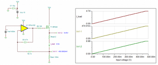
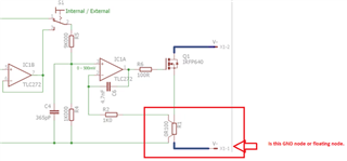
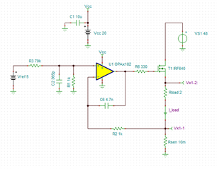
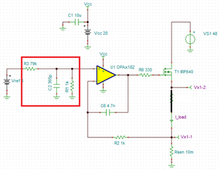
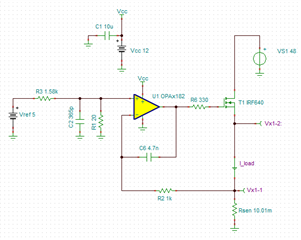
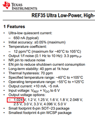
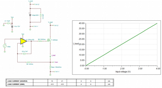
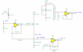
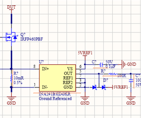
 I am currently working on a high precision, high current electronic load, and I am curious if I use the OPA182IDBVR will I gain more precision in the current setting? The op-amp will be used to sense the current through a 0.1 ohm resistor and an IRFP640 n-channel MOSFET will be used in the linear region to dissipate the required current (maximum of 6.25 amps) set by a voltage on the non-inverting pin of the op-amp. I am basing my circuit around this schematic:

https://community.element14.com/resized-image/__size/1445x452/__key/communityserver-blogs-components-weblogfiles/00-00-00-00-13/8407.contentimage_5F00_59055.png

Since the OPA182IDBVR is different from the TLC272 can I still use the same values for C4 and C6 in the schematic above? If not which values do you recommend I use for the OPA182IDBVR part to keep it from oscillating?

The reason I want precision is I will be commanding up to eight of these "modules" on one board so I can pull up to fifty amps of total current. I want all eight modules to be as close as possible so when I command all eight to turn on at a set voltage I get an accurate total current draw. The electronic load will be used to find the current limit trip points from a new motor controller design and to also test for heat dissipation at rated running current from the input power supply hot-swap circuit. 

Please let me know.

Thanks,

Eric Norton

  • Hi Eric, 

    I know the following simulation is not what you need. I need to sort of a few requirements before I am able to provide a suggestion. You may use the simulation to get some ideas about the V-to-I configuration. 

    OPA182 VtoI Converter 11152023.TSC

    Questions:

    a. With 0.1Ω sensing resistor, the power dissipation on the resistor is still close to 3.9W under a heavy load. As simulation, the constant current is only able to source approx. 4.7A.

    b. The low side of the electrode load is always referenced to GND or it is floating. The feedback is referenced to GND as simulated. If the load is floating, then there will an error in the current source.  


    c. The electronic encounter a capacitive load or complex load. What is the worst case capacitive load that the V-to-I is able to drive in your application? A larger capacitive load will require difference compensation, which is compensate via C6 in this case. 

    d. OPA182 will definitely work better and improve the performance than TLC272. OPA182 is a precision and zero drift op amp, see Vos and Vdrift figures. TLC272 is a general purpose op amp. Under the load current sourcing application, the current errors can be significant. 

    e. We have to perform AC stability analysis and make sure the V-to-I is stable under the max. capacitive or complex load (else you will see oscillations). 

    If you have other questions, please let me know. 

    Best,

    Raymond

  • Hi Raymond,

    Answers to your questions:

    a: Yes I am aware that the sense resistor would dissipate 3.9W at the full 6.25 amps. I am thinking of paralleling four 400 milliohm 2512 SMT resistors together to "share" the load OR go with a 10 milliohm single resistor but then the control voltage becomes very low and then may be hard for the op-amp to control the loop. If by choosing to use OPA182 op amp can it control a range of 0 ~ 0.0625V with reasonable accuracy? You mentioned 4.7 amps. Why is the load limited to 4.7 amps? Is it because of the power dissipation of the sense resistor or is this a limitation of the op-amp or is it the SOA of the MOSFET?

    b: V- will be connected to Ground. I used the circuit pictured as an example. In the final schematic, I will have eight of these "modules" with one common DUT+ and DUT- connection to the load. All eight circuit modules will be on the same board with a large heatsink with a high-speed fan to remove the heat.

    c: I will be testing power supply circuits like a hot-swap controller and also test the current limits of this hot-swap controller. This is why I need the accuracy so I know exactly where the current limits trip and if they are in spec or not. The maximum capacitive load on the boards I will be producing is upwards of 8000 uF maximum. The smaller two-axis boards will have about 2000 uF capacitance there about whereas the larger eight-axis boards are going to have 8000 uF.

    d: Ok great and thought this op-amp looked good :-). I just wanted to make sure it would work well in a high-precision application such as this where I need the precision. I am also going to be using the INA780 or INA781 device to sense the DUT voltage and current. 

    e: For my in-house testing requirements the electronic load doesn't need to be complex and does not need to have a fast response. I am more concerned with trip points and PCB dissipation stress testing.  

    Just to give a bit more information on the overall larger design picture:

    DUT voltage can be up to 80V of course with limits to current with respect to the MOSFETS SOA

    The total current needs to be up to 50 amps. I may need to run high current testing up to 48V but this will be rare and short bursts only. Most of the tests will be at 24V.

    One thing I am struggling to figure out is the voltage reference for all of the ADCs and DACs. Since this electronic load will be a precision instrument, how do I distribute one very tight tolerance 5V voltage reference to all ADCs and DACs? Do I use a high-efficiency buck converter and then adjust the output voltage using a high-precision resistor divider in the feedback and use a very large power plane to reduce voltage drop? How would you tackle this issue? I want to use an ADC and a DAC per electronic load module on the board. The board will be rather large and I don't want to run long analog traces to a central microcontroller because of the voltage drop of the long traces. Instead, I want to use local ADC and DAC so that each electronic load module has the compensated control voltage and the current measurement information sent and received via I2C to the main microcontroller. If this is overkill let me know.

    Thanks,

    Eric Norton

  • Hi Eric, 

    We have some great selection of voltage references in the link below. For instance, REF35REF50xx, REF60xx,  REF70 and many other low cost, low noise, very low drift precision voltage reference for the ADC application.  

    https://www.ti.com/power-management/voltage-reference/products.html#sort=241typ;asc&

    For a precision reference voltage, you may use 5Vref bandgap and/or other lower voltage reference + op amp as buffer for the application. OPA187/OPA2187 are ultra low drift precision op amp and should minimize the Vos and thermal drift errors for the application. Of course, we have many other lower cost zero drift precision op amp for the application.  

    REF35 + OPA187 for Vref 11152023.TSC

    If your application is desired to keep noise down or isolating the noises from the electronic load or switching power supply, you may consider to use our isolated amplifier, such as 

    AMC1311xISO224 or other isolation amplifier families, see the link below. 

    https://www.ti.com/isolation/isolated-amplifiers/overview.html?keyMatch=ISOLATION%20AMPLIFIER

    I will work on your V-to-I constant current source tomorrow. It will be a bit challenge to compensate a lager capacitive load for the topology. I will let you know tomorrow. 

    If you have other questions, please let us know. 

    Best,

    Raymond

  • Hi Raymond,

     Thank you for the reference choices. I will wait for your response tomorrow and hopefully get this project going in the right direction. I have to finish this electronic load design before I can continue working on the laser controller designs. 

    Thanks,

    Eric Norton

  • Hi Eric, 

    The enclosed is the constant current source for the Eload application. I did the minimum changes per your request, increased the phase margins by increasing R6 from 100Ω to 330Ω. You may be able to decrease the C6 from 4.7nf to 1nf range, it will improve the phase margin slightly. 

    OPA182 6.5A Step Transient Eload 11162023.TSC

    Below is the AC analysis and it is stable with phase margin at approx. 80 degrees. 

    OPA182 6A Eload AC Analysis 11162023.TSC

    What types of devices does the Eload use for typically? Is it for general purpose or special application? The low side of current sensing are easier to design, but the noises on the low side may affect the feedback loop. High side current sensing has different pros and cons, so I would like to know that the Eload is designed for what types of application.  

    If the Eload is testing the battery, then it may be ok as is. If the Eload is testing switching power supply or noisy power sources, I would recommend to place a difference amplifier or instrumentation amplifier (IA) across the 100mΩ sensing resistor (to reject the common mode noise better). You may reduce the Rsense to 1-10mΩ, say in IA feedback configuration while keeping the accuracy of the current source, even at the low current scenario (still keep the Rsense on the low side without changing the schematic significantly). 

    If you have other questions, please let me know. 

    Best,

    Raymond

  • Hi Raymond,

     First of all, thank you for all the work you have put into this Slight smile. It is greatly appreciated. Your circuit changes are noted and will get the parts on order to test this. What are these and are they required:

    I see the Cdiff of 3.7pf and Ccm of 2.3pf. I can order these with no problem as well and try it out. Are C3 and L1 required or are they just for simulation purposes? 

    I will be using eight eload circuits with VLOADs tied together to form one large ELOAD circuit on one big board to pull a max of 50 amps current at up to 80V. The ELOAD design will be used for general purposes. Nothing special or fast transient response testing will be done with the ELOAD. 

    I plan on using a high-side current sense like the INA780 or INA781 device BUT NEED SAMPLES. I was declined for the sample program and not sure why. I may just use the discrete version I was planning since it is available to purchase. 

    Please let me know about the components in the attached image.

    Thanks,

    Eric Norton

  • Hi Eric, 

    The captured image is a part of dual feedback AC Loop Analysis. It is not required in a real circuit.  I included the common and differential mode input capacitance when the input loop is broken for the loop analysis, see the video clip in detail. The video clip is posted over youtube.com, but series of these video clips trainings can be found in ti.com, which different topics are well organized.  

    If you open the AC analysis, I have included in the simulation files about the common and differential capacitance at the inputs. 

    https://www.youtube.com/watch?v=L6ecVTDJ2-4

    You should be able to order samples via the link below, but I do know that it will take time, even for us. Alternatively, you may contact our FAE in your area, which they have to a way to provide you sample at much faster pace. 

    https://tisamples.ti.com/order/tisamples/en/

    If you have other questions, please let me know.

    Best,

    Raymond

  • Hi Raymond,

     If I use a lower Rsense resistor, will the OPA182 device work at that low of a control voltage? I thought about using an amplifier but then that would introduce a delay or am I wrong? I simulated something similar to this idea but when it came time to test it in real life it oscillated like crazy. Any ideas?

    Thanks,

    Eric Norton

  • Hi Raymond,

     Oh ok, I will disregard the AC components then and take a look at the YouTube video to learn more about it. Since the INA780 devices are hard to get I will go with a discrete version I have been working on with a localized I2C ADC. Kind of clunky to be honest but it will work. I'd like to use the ADC on my microcontroller but don't want to route analog traces twelve inches from the DUT voltage buffer and current sense amplifier. There would be too much voltage drop and it would be inaccurate by the time the signals reached the microcontroller. With digital I2C I can send the data over a distance with no issue.

    Thanks,

    Eric Norton

  • Hi Eric, 

    Could you send me the schematic? I will see If I am able to compensate for it. 

    The input common mode range for OPA182 is shown below, and it should work for the low side V-to-I converter sensing application. 

    If you prefer to keep the schematic private, please send me a "friendship" request via E2E forum, and we can discuss these topics in private messaging. Or I can provide you with my email and we can discuss via email as well. 

    Best,

    Raymond

  • Hi Eric, 

    The current sense monitor is supported by our sensing team, and I do not work on these products. I am in Precision Op Amp Application Team, and the most of PRAMPS products in this team are analog in nature.

    If you want to know more about INA780 performance and availability, please contact the sensing team over the E2E forum. 

    Best,

    Raymond

  • Hi Raymond,

     All I have at the moment is the schematic I provided in the first message. I went on to the most current design since the last one didn't work Disappointed. Ideally, I'd like to use a Rsense that won't dissipate much power so that all the dissipation is in the MOSFET only. What simulation software do you use? Is it something I can download and use? Please let me know.

    Thanks,

    Eric Norton

  • Hi Raymond,

     Oh, ok, no problem. I will reach out to them and see if I can get anywhere.

    Thanks,

    Eric Norton

  • Hi Eric, 

    You can download TINA-TI simulator tool for free in our websie, see the link below. This is the same simulator that we use it as well.  

    If you use other vendor's simulation tool, you are able to import our spice op amp model and it will work as well. 

    https://www.ti.com/tool/TINA-TI?keyMatch=TINA%20TI%20DOWNLOAD

    If you have other questions, please let me know. 

    Best,

    Raymond

  • Hi Raymond,

     Thank you for sharing Slight smile. Is the OPAx182 device part of TINA? I can't find it for some reason. If it isn't part of TINA do you have the SPICE model?

    Thanks,

    Eric Norton

  • Hi Eric, 

    The x in OPAx182 is the part of op amp naming system for single, dual quad package. Here is the link and all the models are shown in the same.  

    https://www.ti.com/product/OPA182#design-tools-simulation

    Best.

    Raymond

  • Hi Raymond,

     I downloaded your design and tinkered a bit. I came up with this:

    I decreased the Rsense to 10 milliohms instead of the 100 milliohm resistor and total dissipation at 6.25 amps is ~0.39W. I also added the resistor divider of 79k and 1k and threw in the 365pF capacitor as well and I indeed got the 6.25 amps I need when I run the DC analysis. I also noticed the limit of 4.7 amps was due to the 15V applied to VCC. I raised it to 20V and can now get the full span I am looking for. Now the question I have will this work without it oscillating like crazy? Let me know your thoughts.

    Thanks,

    Eric Norton

  • Hi Eric, 

    Please remove 2Ω load between IRF640's source and Ground. I was not sure how you are going to connect the load yesterday, so I placed one as shown in the schematic. IRF640 mosfet is your load now. With 2Ω load, the mosfet's linear region is limited. 

    If you have other questions, please let me know. 

    Best,

    Raymond

  • Hi Raymond,

     Ah, ok, thanks for that. I was wondering what that was there for. Do my modifications look correct to you? Do you think this would work? I have to find suitable values for the resistor divider that are available through a distributor with very tight tolerances so that will be a chore in and of itself lol. Let me know your thoughts.

    Thanks,

    Eric Norton

  • Hi Eric, 

    This should work. 

    The non-inverting input has a LPF, and I think that you want to have the cutoff frequency is sub 100Hz range, where fp = 2*pi*(R3||R1)C2. 

    With the low dc input voltage signals, it would be better off to have DAC configuration at the input (use low Vref for DAC to maintain the bit accuracy, also you may be able to change the setting readily). The resistor tolerances and voltage divider may create to larger errors and variabilities for the application. 

    If you have other questions, please let me know. 

    Best,

    RAymond

  • Hi Raymond,

     I changed the resistor values for the input divider:

    If I use 0.1% tolerant parts for the 1.58k and 20 ohm resistors then the variance between parts is negligible and I can live with it. I thought about using a DAC that goes straight into the op-amp but trying to find a 0.0625V accurate voltage reference or designing a precision Vref that low would be hard unless you know of a way that I haven't thought of. Any slight variation of Vref would reflect on the output of the DAC and then also have to factor in the DAC error. I can get Vref of 5V that are very accurate and they are a bit pricey but easier to handle with such a wide voltage the error plus the tolerance would not transfer much to the output or am I wrong in my thought process? Please let me know. Btw, thanks for your continued help with this. It is much appreciated.

    Thanks,

    Eric Norton

  • Hi Raymond,

     I am still new to TINA and trying to find my way around the software. How do I check the current flow through the 330-ohm resistor at a full Vref of 5 volts? I want to size the resistor so that it is big enough to handle the current going to the gate of the MOSFET. Please let me know.

    Thanks,

    Eric Norton 

  • Hi Eric, 

    Please check out the Tina-TI video training clips.  

    https://www.ti.com/sitesearch/en-us/docs/universalsearch.tsp?langPref=en-US&preFilter=video&searchTerm=tina-ti&nr=169#q=tina-ti&sort=relevancy&numberOfResults=25&f:videos=[Video,Video%20series]

    In terms of low voltage reference, REF35 has 1.024Vref, which is reasonably priced with good temperature coefficient. If you use 12bit DAC, then the bit resolution will have approx. 1.024V/2e12 bit = 250 uV/bit.

    Please ask for DAC support team for a low cost, low voltage DAC for your application.  

    How do I check the current flow through the 330-ohm resistor at a full Vref of 5 volts?

    You should perform hand calculation with the simulation. The simulation is not always correct. 

    Best,

    Raymond

  • Hi Raymond,

     Thanks for the information. I will look into all of this and let you know if I need further assistance. 

    Thanks,

    Eric Norton

  • Hi Eric, 

    Ok. TI's video series have tons of different learning topics, and it is informative.

    Please let us know if you have other questions. 

    Best,

    Raymond

  • Hi Raymond,

     Okay, so I have good news to report. I received the new parts for the electronic load and soldered everything up, and to my surprise, it works flawlessly. I tested up to 4 amps thus far and it tracks properly. I would test up to the full range, but I don't have a power supply that can handle 6.25 amps wired up yet. THANK YOU SO MUCH for all of your help with this. Mucho appreciated Slight smile.

    Happy Thanksgiving!!

    Thanks,

    Eric Norton

  • Hi Eric, 

    Good to hear that the circuit is working. 

    If you have other questions, please let me know. 

    Happy Thanksgivings!

    Raymond

  • Hi Raymond,

     Sorry for the long delay Disappointed. I had an emergency but all is well now. Thanksgiving was great and hope yours was too. Not sure if you can shed some light on this subject but want to use the REF02B reference chip to power an MCP3221 ADC and MCP4725 DAC. I am looking at the REF02B datasheet and I see stars in the REF02B section under the electrical specifications. Do the stars mean they are the same as the REF02A device? I am a bit confused by this. Both the ADC and DAC draw uA of current even in active mode and that is all that will be powered by the REF02B device. Let me know your thoughts on this Slight smile.

    Thanks,

    Eric Norton

  • Hi Eric, 

    Do the stars mean they are the same as the REF02A device?

    You could assume that they are the same. REF02B is higher grade than REF02A, which REF02B has tighter performance specification. The "*" implies as typical, which is one standard deviation among a large sample population. In manufacturing process, only REF02A performance specification is screened; and the better performance specification goes to REF02B or higher grade bucket.  REF02A and REF02B are from the same IC dies, tighter min and max. ranges are classified as REF02B grade, and samples with slightly wider ranges are classified as REF02A grade. Outside of these ranges are discarded.  

    If you have other questions, please let me know. 

    Best,

    Raymond

  • Hi Raymond,

     Ah, okay well the REF02B is a good choice then. So is it safe to assume the output current is 21mA for the REF02B part? Is it possible to use a digital potentiometer to do a digital calibration of the TRIM pin? Is there a high tap count digital pot that is higher than 1024 or is this the highest they go? I want the output of the REF02B to be exactly 5.0000V or as close as it can be within reason since I will have eight of these load circuits on one board connected to the main DUT + and need each of them to be the same voltage.

    On to another op-amp topic. I have another part of the electronic load circuit and I will have a voltage divider to step down the range of 0-80V down to 0-5V range. I'd like the op-amp to be as accurate as possible in a "buffer" follower configuration. Can I use the same OPA2182 (OPA182 will be used in the final design) series for this and do you have a recommended circuit for this? I'd also like to protect the op-amp input from high voltage in case the voltage divider fails. I thought of a way to do a bootstrap diode on the input and then use Schottky diodes and some resistors on the output or would that weigh down the output by doing this? What do you recommend I do? I need the buffer follower circuit to be as precise as possible with no error/offset from the input to the output voltage. This circuit will measure the DUT voltage and I will be making decisions based on the DUT voltage and current so it needs to be precise as possible. 

    Thanks,

    Eric Norton

  • Hi Eric, 

    So is it safe to assume the output current is 21mA for the REF02B part?

    If you pick a low Vos precision op amp, you should be able to double or even triple the source/sink current up to 60mA ranges. 

    Of you can make up one op amp buffers at 5.000V and share the single op amp buffer output with several nodes, say 2-4 nodes depending the output current requirements. You may use one bandgap reference and feed into multiple op amp buffers for this configurations. 

    I will have a voltage divider to step down the range of 0-80V down to 0-5V range. I'd like the op-amp to be as accurate as possible in a "buffer" follower configuration.

    If you want to obtain close to 5.0000V high voltage precision, the voltage divider step down from 80V is not good ideas. You will need to have very precise 80Vdc and require voltage trim to obtain the precision. Temperature variations could interfere with the precision voltage. 

    I mentioned previously, use DAC to configure your Vref voltage. 

    In our power amplifier, we have OPA593, which it will be good to amplifier to work in this application, if the load current is not high. If you are concerned about about the power efficiency, then you have to use switching power supplies or buck converter or IC to step down the output. 

    https://www.ti.com/lit/ds/symlink/opa593.pdf?ts=1701387059006&ref_url=https%253A%252F%252Fwww.google.com%252F

    If you have other questions, please let me know. 

    Best,

    Raymond


  • Hi Raymond,

     Okay, I think I might not have explained the situation clearly. I will be using the REF02B as a low-current power supply for an I2C DAC and ADC which do not have reference pins. I will use one REF02B chip per electronic load circuit (there are a total of eight electronic load circuits on the board). All eight of these load circuits will all work together to pull a total of 50 amps of current from the DUT (device under test) hence the 6.25 amps of current limit I have been talking about through our conversations. The reason why I want to do eight electronic load circuits is because of the SOA of the MOSFETs. I don't want to use a single MOSFET to handle 50 amps of current at up to 80V. If I use a single REF02B with a current amplifier I will still have a voltage drop because the board will be large and any voltage drop is no good for this precision application. This is why I want local references close to the load circuits so that they are very precise.

    The second question was about the 0 to 80V DUT (device under test) voltage divider and using an op-amp in a buffer/follower configuration so it doesn't load down the ADC. I am going the discrete component route because the INA780 device is not available and need to get this electronic load project done now. I need to measure a voltage range of 0 volts to 80 volts and a current range of 0 to 50 amps and I am doing it using discrete components and two I2C ADCs. 

    Hopefully, this clears up any confusion about what I am trying to do. 

    Thanks,

    Eric Norton

  • Hi Eric, 

    You'd like to use REF02B ref voltage + digital potentiometer to replaced Vdac voltage reference in your application.

    BTW, you can not assume REF02B is capable to source 21mA, which is typical. The worst case is 10mA in the part, which this is one you should consider as the source current ratings.  

    I realized that the output current per IRF640N is approx. 6.25A/channel, so Vdac is only ranged from 0V to 625mV. If my understanding is incorrect, please include the drawing, block diagram or schematic of the design requirements. 

    I do not support our digital potentiometer product lines. From what I see, TI seems to have up to 256 bit resolution of digital pots. If you found 1024 bit type, that is probably the high end of the product line, see the TI's link below. 

    https://www.ti.com/data-converters/digital-potentiometer/products.html?keyMatch=DIGITAL%20POT#

    Since Vdac in the V-to-I has to be very precise, I do not think that the voltage divider approach is accurately enough. How many current settings do you need in your Eload?

    If you use REF02B, and replace Vdac with DAC's output, then you should have more precise input voltage control. 

    I need to measure a voltage range of 0 volts to 80 volts and a current range of 0 to 50 amps and I am doing it using discrete components and two I2C ADCs. 

    INA780 is available in TI E-store, but the qualities may be limited.

    https://www.ti.com/product/INA780A?login-check=true#order-quality

    To measure 0-50A and 0-80V range, you may consider the following circuit. I assume that the common mode noises are minimum. If GND is noisy, then you may consider to implement differential input measurement.  

    OPA182 6.5A Step Transient Eload 12012023.TSC

    If you have other questions, please let me know. 

    Best,

    Raymond

  • Hi Raymond,

     The INA780 shows out of stock Disappointed

    The REF02B will be used to power the ADC and the DAC. Both devices are micropower devices and will not even come close to the 10mA or 21mA current draw of the REF02B device.

    Okay, I will use a multi-turn potentiometer to trim the REF02B devices.

    I will draw up my schematic in Altium and when I have a circuit I will share it with you to confirm I am doing things right Slight smile. Thank you for your help as always. I'll be back hopefully in the next few days with something for you to look at.

    Thanks,

    Eric Norton

  • Hi Eric, 

     The INA780 shows out of stock

    I see, Please speak to current sensing team, they will find alternative high side current sensing monitors for 85V or higher application.

    Best,

    Raymond

  • Hi Raymond,

     Okay, will do! By the way, I am going to use this device to sense across the 10-milliohm resistor: INA241B3IDGKR. Is this overkill? It has a gain of 50 which if I have a range of 0 to10 amps (0 to 6.25 amps max with a little headroom) per electronic load circuit then a gain of 50 would be perfect for a scale of 0 to 5 volts. Let me know if I am on the right track.

    Thanks,

    Eric Norton

  • Hi Eric, 

    It certainly looks that INA241B3IDGKR will work for the application. It will not be an overkill, if it meets your Eload requirements. It has excellent CMRR, which the application may need. 50V/V fixed gains are good choices for the application. in terms of pricing, it is not overkill at all. If you have to implement the discrete current sensing difference amplifier approach, the design part counts will cost more. 

    Anyway, please talk to the CS team about the implementation. I think that it could be a good choice for the application. 

    Best,

    Raymond

  • Hi Raymond,

     Okay, great Slight smile. Here is one of eight EL circuits:

    This will give you an idea of what I am thinking about doing. All eight circuits will pull a collective current from the DUT (device under test). The microcontroller (not pictured) will have three I2C masters controlling the eight DACs, and eight ADCs and also controlling the DUT voltage and current measurement circuits. I hope this helps clarify my goal here. Let me know if the component selections look ok and if you recommend any buffering or component changes Slight smile.

    Thanks,

    Eric Norton

  • Hi Eric, 

    Ok, I will take a look next week. 

    Best,

    Raymond

  • Thank you Raymond. Have a good weekend!

  • Hi Eric, 

    Here is the application note for replacing digital potentiometer with a precision DAC.

    https://www.ti.com/lit/an/slaa906/slaa906.pdf?ts=1701566650326&ref_url=https%253A%252F%252Fwww.ti.com%252Fproduct%252FTPL8002-25

    You mentioned that you want to keep the accuracy as high as possible, and I think that DAC will be the way to go. If you'd like to use digital potentiometer, then you need to check out the worst case errors at your input. You have not defined how accurate or %errors you want in your Eload, Perhaps, the digital potentiometer is good enough for your application.   

    I do nor work with INA241 CS monitor. Please make sure that it will operate at 5V in a single supply rail with Vref1=Vref2=GND. 

    In addition, it would be nice to use INA241 to feedback the part of Rsense shunt (10mohm) back to the op amp. The output of INA241 will reject the most of common mode noises. If the GND noises are excessive (like high frequency switching power supply), then you should tap into INA241's output for both ADC and part of voltage feedback. 

    If you have other questions, please let me know. 

    Best,

    Raymond

  • Hi Raymond,

     Thanks for the information. As you can see in my schematic I will use the potentiometer as shown to trim the REF02B part. As the schematic is drawn, I incorporated the changes we have been working on together. I also included TI DAC to control the op-amp stage and an ADC to measure the current off of one of eight of these "electronic load modules". I want to keep the feedback from the sense resistor going into the op-amp because I tried to use a current amplifier before and it didn't work. The circuit oscillated like crazy. I want the ADC there so that I can fine-tune each of the eight electronic load modules and also make sure the circuit is working properly. 

    I just wanted to run the complete circuit by you so you can see what I intend to do and get your professional opinion on whether it will work as drawn and any recommendations for component changes. 

    The INA241 datasheet says 2.7 ~ 20V operation so 5V should work. 

    Any ideas or recommendations welcome Slight smile.

    Thanks,

    Eric Norton

  • Hi Eric, 

    The INA241 datasheet says 2.7 ~ 20V operation so 5V should work. 

    I do not work with INA241 daily so it will be good to check with CS application engineers. Yes, I agree that it should work. These device has certain ranges of Vcm vs. Vout that is operating linearly. So you should check it out. 

    The circuit oscillated like crazy.

    I thought that the V-to-I circuit oscillation is resolved and working. Are you talking about a while back?

    Best,

    Raymond

  • Hi Raymond,

     Ok, I will talk to someone in the CS. 

    Yes, the V to I circuit is working properly. I was referring to what you mentioned in your last message about using the INA241 for feedback to the op-amp and

    to the ADC. I did try something similar to what you are talking about and it oscillated like crazy. That is when I came asking for help with this and you have helped me resolve my issues. I just want to make sure what I have drawn up in the schematic will work properly before I lay out a board and put it together.

    Thanks,

    Eric Norton

  • Hi Eric, 

    It would have worked, if the entire feedback loop is compensated properly.

    If you have other questions, please let me know. 

    Best,

    Raymond