This thread has been locked.

If you have a related question, please click the "Ask a related question" button in the top right corner. The newly created question will be automatically linked to this question.

OPA855: OPA855 Circuit Analysis and Debugging

Part Number: OPA855
Other Parts Discussed in Thread: LMH6624, OPA859

Hi, 

The Great thank for suggesting OPA855.

Trailing from 

LMH6624: LMH6624: LMH6624MAX NOPB amplifier noise reduction when used to measure the current with shunt. - Amplifiers forum - Amplifiers - TI E2E support forums

I used OPA855 on same board with all correction from above conversation.

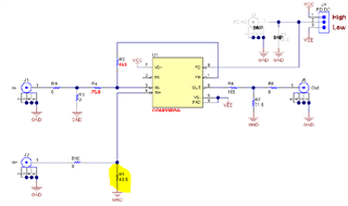
PCB assembled as per EVM circuit --> OPA855IDSGEVM , app note--> sbou210, all values matches with EVM circuits recommended values. 

R6 = 0E, R7 = Not assembled (It was giving zero output), First OPAM output connected directly to second, and so on. All other components used as it is. 

No oscillation at output of any OPAM observed as seen previous with IC LMH6624. (I think this OPA855 working fine) and taken below readings. 

3 OPAM working fine in series. 

Input voltage is 20mV AC 25MHz.

IC VCC = 2.2V, VEE = -2.2V. Input signal is taken from 

When assembled fourth OPAM --> output is not acceptable. 

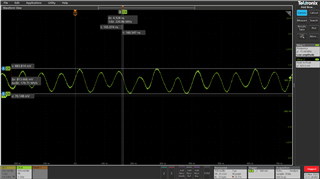
OPAM 1 OUTPUT.

OPAM 2 OUTPUT.

OPAM 3 OUTPUT.

OPAM 4 OUTPUT.

Q1- what can be reason that OPAM 4 is saturated? Even when input voltage 1mV AC 25MHz. (Input voltage is given form function generator. Function generator output voltage is nearly accurate.)

Q2- why AC signal shifting by adding some voltage?

Q3- why gain calculation of EVM, not matching with results. Even I checked EVM, for one OPAM output, result is same. 

  • Hi Anurag,

    From the screenshots of the opamp outputs you provided, it appears that the signals are not clean signals. Can you share how you are measuring the outputs of each opamp?

    Can you clarify a few things about your circuit:

    1. What is the voltage being applied at Vin+?

    2. When you say that you designed the board with the OPA855IDSGEVM values, are you referring that Rf is 453 ohms and Rg is 75 ohms for each opamp stage?

    3. Can you share the PCB layout that you are using for the 4 stage amplifier?

    These will help to understand why you are seeing these behaviors.

    Thanks,

    Nick

  • Hi Anurag,

    Thank you for providing the additional information. To answer the questions you posed previously:

    1. The OPA855 has a DC offset voltage of approximately 2mV. This is getting gained through every stage and this is why you are seeing the DC offset on the output of each op amp continue to increase. By the fourth op amp stage, the DC offset is beyond the output swing limitation so it will be saturated at the output swing limit.

    2. See above answer

    3. It is not clear why the expected gain of 7V/V is not being met. Can you send a PCB layout for the OPA855 design that you are using with the multiple op amp stages? Understanding the current layout you are testing will help to troubleshoot why the gain is not what is expected.

    Can you confirm this schematic matches what you are testing?

    Are you able to elaborate on what output voltage/gain are you expecting for your application? It is possible to use the OPA859 in a unity gain configuration after the first two stages so that you can set the gain at 1V/V for the later stages.

    Thanks,

    Nick

  • Hi,

    I have this R1 49.9 Ohm connected in each OPAM stage. When I disconnected from first OPAM, circuit was not working, so I kept in each stage. 

    Is it impacting results?

  • Hi,

    When 3 mV offset added to input, it works fine. At output no offset comes as seen earlier.

    + OPAM 4 Gain changed to 2 --> to make output voltage within range of 2.2V.

    It seems working fine now.

    But now what I observed that, If I change the input signal frequency from 1MHz to 25MHz --> output voltage gain changes.

    As it is high bandwidth OPAM, I think It should work for 25MHz.

    ---------------

    Same observations on EVM, But its voltage goes little low for 25MHz than 1MHz.

    ---------------

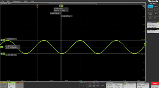
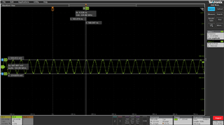
    Below are EVM results.

    ---------------

    Input voltage 200mV = Vin, 1MHz (But when I measure voltage across R1, it comes 152mV pk-pk)

    ---------------------

    Input voltage 200mV = Vin, 25MHz (But when I measure voltage across R1, it comes 120mV pk-pk)

    ----------------------

    What is the significance of R1 in EVM schematic?

    -----------------------

    -----------------------

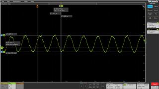
    Below are the waveforms taken on my board.

    Input Vin = 2mV

    Gains are 7, 7, 7, 2

    At 1MHz

    -----------------

    At 15MHz, and signal getting worse.

  • Hi Anurang,

    R1 is a termination resistor to match the impedance of the voltage source. You should include R1 on the first stage with a value that matches the impedance of the input voltage source. However, including R1 on the subsequent stages will induce a voltage drop as that would create a resistor divider network.

    My assumption is that the last two waveforms you have provided are being measured on the output of the fourth stage amplifier. If this is the case, I would expect the results you are seeing since the OPA855 is not stable for gains less than 7V/V.

    Can you check what the output of the third stage amplifier is? I would expect this to be a good signal. If you need one more stage to amplify the signal more, I would recommend using the OPA859 for the fourth stage as it is stable for a gain of 2V/V. 

    Thanks,

    Nick

  • Last two waveforms are taken on my designed board with frequency 1MHz and 15MHz.

    First two waveforms are taken on EVM with frequency 1MHz and 15MHz.

  • Hi Anurag,

    Thank you for providing the clarification. A few observations that I have:

    1. The waveforms you provide using the EVM indicate a gain less than 7V/V. Can you confirm that you are still using an Rf of 453 ohms and Rg of 75 ohms? Can you also confirm if that is just one stage?

    2. The waveforms you provide for the board you designed indicate instability which I would expect with the last stage having a gain of 2V/V. Are you able to provide the output voltage of three stages set at a gain of 7V/V and input voltage of 2mV (i.e. remove the fourth stage that has a gain of 2V/V and measure the output voltage after the third stage)?

    Thanks,

    Nick

  • 1. The waveforms you provide using the EVM indicate a gain less than 7V/V. Can you confirm that you are still using an Rf of 453 ohms and Rg of 75 ohms? Can you also confirm if that is just one stage?

    --> yes using same values as EVM. I think 50 E at input dropping input voltage. 

  • Hi Anurag,

    Can you confirm that you are driving the input with a 50 ohm impedance input source? If the input source has a different impedance, the input will not be properly matched and you will see reflections that will result in distortion or instability.

    Thanks,

    Nick