Because of the Thanksgiving holiday in the U.S., TI E2E™ design support forum responses may be delayed from November 25 through December 2. Thank you for your patience.

This thread has been locked.

If you have a related question, please click the "Ask a related question" button in the top right corner. The newly created question will be automatically linked to this question.

INA190: Transient protection and layout

Part Number: INA190
Other Parts Discussed in Thread: TVS2700, ,

In order to provide context, I will use the INA190 as a 4-20mA receiver, and I have concerns about how to protect its inputs. The idea is to use it in Loop Current mode. The power supply for the sensor is provided from the host card, reducing the risk of reverse polarity. The maximum voltage for the sensor's power supply is 24V.

For the selection of a TVS diode, I have read the following article

How to select a surge diode

According to the reading, I believe the TVS2700 fits my requirements

TVSxx00

The Vrwm is slightly higher than the nominal operating voltage of the sensor, and the clamping voltage is lower than the maximum Vcm supported by the INA190 (40V max). Additionally, the leakage current is very low: 1.7nA

According to the question found at the following link

https://e2e.ti.com/support/amplifiers-group/amplifiers/f/amplifiers-forum/1255372/ina190-transient-protection?keyMatch=INA190%20TRANSIENT

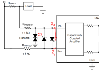
I have doubts about how to connect the TVS2700. In the following diagram, the Transorb is highlighted in red. Correct?
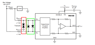
What part number could I use for the elements in green? What would be the selection criteria?

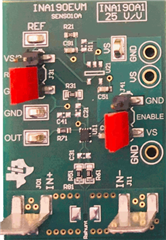
Additionally, regarding the layout, I found the INA190EVM usage guide, where a poor ground plane around the INA190 is noticeable
I also found the usage guide for INA190EPEVM. There is no photo of the  PCB, but the existence of a ground plane is observed on the top layer of the gerber.
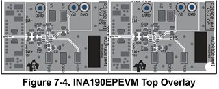
The packages are different. Should a ground plane be applied for the SOT23 (8) version? 

Thanks in advance

  • Hello Valued Engineer,

    The elements in green are just simple rectifying diodes (in a "series-pair" package). The reason for this is that it allows you to only need one of the tranzorbs for both IN+ and IN- pins (as opposed to two tranzorbs one for each pin). This works because if IN- pin goes to > 42V, then IN+ pin will be clamped as well because one of the diodes will become forward biased and vice-versa. I had recommended this series pair diode package in last post: https://www.digikey.com/en/products/detail/skyworks-solutions-inc/SMS7621-006LF/2052129

    There is a ground plane for the INA190EVM on the bottom layer as seen in the User's Guide Figure 7.

    Ideally, all integrated circuits should have large ground planes (and supply planes as well). This theoretically will always help minimize parasitic impedance into the supply pins and provide other benefit such as noise protection. This is especially true for circuits requiring significant amount of switching current. The INA190 is a low power device so parasitic impedance into VS pin and out of GND pin is not overly critical. The EVM was designed to keep in mind that realistically a designer cannot always provide large ground planes and provide opportunity to demonstrate performance without them.

    Overall, all you can do is to make sure the ground return trace for INA190 is not long/thin/inductive and returns to a low-impedance and stable ground. Down-stream signal measurements of INA190 OUT should also be connected to the same ground to minimize ground level offsets.

    Sincerely,

    Peter

  • Hi Best Regards

    Thanks for reply.

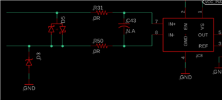
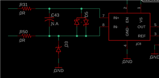
    What do you think is the best components place ? 

    Firts the transient protection

    Firts the filter option

  • Hey Jhon,

    The best option depends upon how much energy you need D3 (reverse DC current) and D5 (forward DC current) to dissipate during system voltage surges.

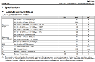
    Maximum current/power ratings are shown in the Absolute Maximum Ratings table for various IEC standards.

    However, if you are tying to clamp a DC voltage, then you need to limit D3 reverse current to 10 mA (see the IBR spec in table above).

    Using the schematic below, you ideally want Rprotect to be as low as possible to avoid input offset error from reverse leakage currents flowing across Rprotect; however, you need Rprotect to limit diode reverse current if need be. TVS2700 reverse leakage is fairly low, but the INA190 offset is also very low so this value should be chosen carefully. The approximate offset error due to leakage (in the schematic below) is Vos_leak = I_lead * Rprotect.

    RF acts only as an input filter here, but it does not contribute to diode leakage offset error. The downside is that you need two more passive components in your BOM.

    One additional advantage to RF in this topology is that it adds some additional protection to INA190 input pins during negative voltage conditions (VBUS <-0.3V) where tranzorb becomes forward biased at around -600mV.

    You could remove RF if you do not need any differential shunt voltage filtering (noisy load current) or system will not experience negative voltage surges (VBUS <-0.3V)/

    CF should always be placed as close as possible to IN+ and IN- pin, regardless of the topology you choose.

    Hope this helps.

    Best,

    Peter