Because of the holidays, TI E2E™ design support forum responses will be delayed from Dec. 25 through Jan. 2. Thank you for your patience.

This thread has been locked.

If you have a related question, please click the "Ask a related question" button in the top right corner. The newly created question will be automatically linked to this question.

OPA818: Reviewing two circuit using OPA818 as a TIA and OPA843 as a Op-Amp

Part Number: OPA818
Other Parts Discussed in Thread: OPA657

Dear Engineers,

I want to make a circuit design for LiDAR receiver application.

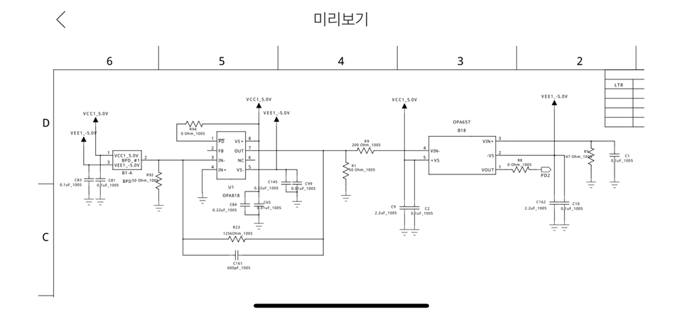
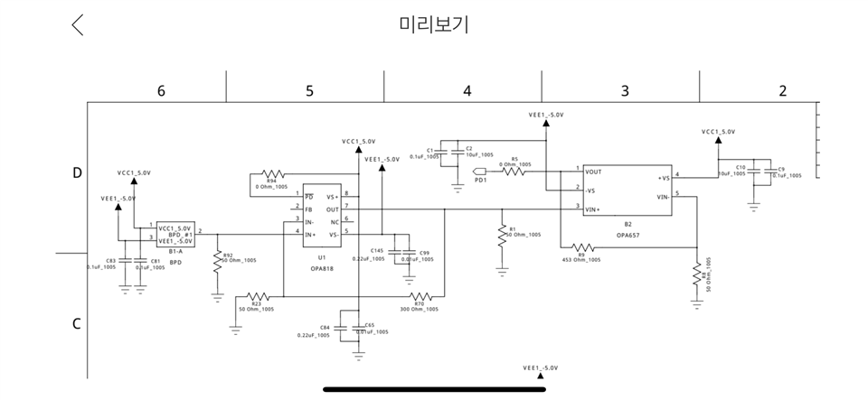
I made a first circuit as a first photo below, but it doesn’t work properly. So I hope to listen to your comments.

please review my two circuits shown below

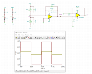
The second design is what I got from the forum as below.

and I hope somebody let me know the reason why second circuit has a inverter function.

my previous post
https://e2e.ti.com/support/amplifiers-group/amplifiers/f/amplifiers-forum/1267024/opa657-device-recommendation-with-tia/4814120?tisearch=e2e-sitesearch&keymatch=%20user%3A572902#4814120

  • Hi Seongjin, 

    I have a few questions about your first circuit:

    1. You mention that the circuit is not working properly. Can you share what your circuit requirements are (i.e. output voltage of first/second stage, bandwidth, etc.)? And what issues are you seeing with the circuit?
    2. Is there a reason that the first stage is not configured as a TIA?

    To answer your question about the second circuit: the reason that the output is inverted is because you are applying a signal to the inverting input terminal (Vin-) of the second stage. If you applied the output of the first stage to the noninverting input terminal (Vin+) of the second stage, the output would not be inverted.

    A question about your second circuit: On the second stage, is there a reason that you have no feedback path between the input and output?

    Thanks,

    Nick

  • Dear Nick Nauman

    Thank you for your comments

    I leave my answers to your questions

    1. This answer is related to question number 2. the OPA818 on the 1st stage should have been designed as to TIA but now I can now know It was designed like operational amplifier. my circuit requirements need to get 250kV/A through the 1st TIA and 2nd Op-Amp. stage.

    2. It was my mistake. I am going to change its design to TIA as described in the datasheet.

    And regarding "A question about your second circuit", I will apply feedback path to my 2nd circuit.

    Thanks!

  • Hi Seongjin,

    Based on your answers, I would recommend a circuit similar to the one I show below:

    I selected the feedback capacitance using the TI TIA Calculator (here). This is assuming a feedback resistance of 25kohm and input capacitance of 13pF. The calculator recommends a feedback capacitance of 250fF, but I selected 500fF as this is more easily realized in hardware under the assumption you did not need a full 36MHz of bandwidth.

    Feel free to make any adjustments based on your application needs. Please reach out if you have further questions.

    Thanks,
    Nick

  • Dear Nick Nauman,

    I appreciate your circuit drawing and simulation.

     I have something to be concerned as below.

    On the first stage with OPA818, the 500f capacitor(C1)  was used.

    the capacitor I have found is too big to use. it size is 83mm which is not suitable.

    So  I hope to use small capacitors such as 0603 for Surface Mounting Technology(SMT).

    For this, If OPA818 has to be changed to use small capacitors, I can consider it.

    In addition, the datasheet of OPA657 shows that Vcc and Vee lines have capacitors for Op-Amp. design

    But your drawing does not. Is it okay for Op-Amp performance?

    Please review my inquiries once more.

  • Hi Seongjin,

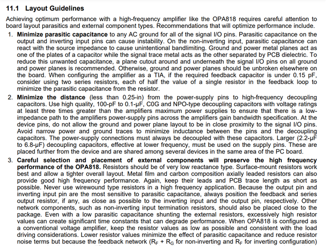
    As you stated, small capacitors are the better choice compared to large capacitors as it allows for a tighter layout which helps reduce parasitic capacitance that can cause instability. This is discussed in section 11.1 part 3 of the layout guidelines, as shown below.

    Also, you should use decoupling capacitors on the supply lines as discussed in part 2 of the layout guidelines. I did not include them in my simulation as those are ideal sources so adding the supply decoupling capacitors would not change the simulation results. However, in the real designs, they should be included.

    I hope this clears up your questions.

    Thanks,

    Nick

  • Dear Nick Nauman,

    Thanks for your quick reply.

    What I understood from your references is how to keep the devices' performance stable.

    I will keep in mind when I design my circuit.

    Additionally, I'd like to know the other way in case  I can't use 500f capacitor in my circuits.

    Actually, the size(83mm) of 500f capacitor is almost the same as my circuit length.

    So if there is a way to get 250kV/A through the 1st TIA and 2nd Op-Amp. stage. without using 500f or similar size of capacitor,

    I'd like to know that.

    For instant, such as reducing gain of 1st stage and increasing 2nd stage gain.

    I always thank for your valuable reply.

  • Hi Seongjin,

    There are a couple options for you:

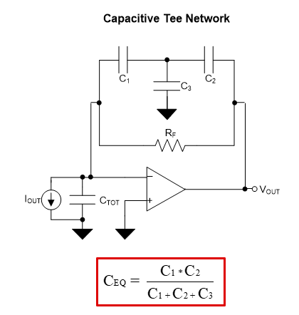
    1. You could use a capacitive T-network to realize smaller capacitor values using a few larger capacitor values. This way you can use a smaller capacitor package instead of the large package option you have currently

    2. You could lower the gain on the first stage and increase the gain on the second stage. Something to keep in mind, by increasing the gain on the second stage, you are lowering the bandwidth on the second stage; therefore make sure not to increase the gain so much as to limit bandwidth. 

    If you decide to change the gain on the stages, make sure to use the TIA calculator I linked above in order to recalculate the feedback capacitor value of the first stage to achieve stability.

    Thanks,

    Nick

  • Dear Nick Nauman,

    I am confused because it seems like that "Capacitive Tee Network" is a method for making total capacitor values smaller.

    But the circuit design that I saw in the previous post has a 500f capacitor for the 1st stage gain.

    So Let me get this clear. Does 500f mean 500 femto Farad? or literally 500 Farad?

    Thanks

  • Hi Seongjin,

    I apologize for causing some confusion. 500fF (or 500f) is 500 femtoFarad capacitor. You should be able to find a small package size capacitor for this value. However, if you are having trouble finding a 500fF capacitor, you can use a T-network to achieve the same result. For example, you could set C1=2pF, C2=2pF, and C3=4pF.

    Using one feedback capacitor will reduce the parasitics of the board, however the T-network can be used if it is not practical for you to use one feedback capacitor at the cost of additional parasitics.

    I hope I have made this clear.

    Thanks,

    Nick