This thread has been locked.

If you have a related question, please click the "Ask a related question" button in the top right corner. The newly created question will be automatically linked to this question.

XTR111: xtr111 external mosfet Vgs ths value selection. gate and input capacitance.

Part Number: XTR111
Other Parts Discussed in Thread: TINA-TI

Hi! I want to select the xtr111 external mosfet Vgs ths(max) value. This value is Vgs ths(max) @ Id 2.5V 3V and 4V. Is it better for this value to be wide or to be in a narrow range? In the datasheet, it is stated that the positive supply rail of the gate can operate up to 16V.

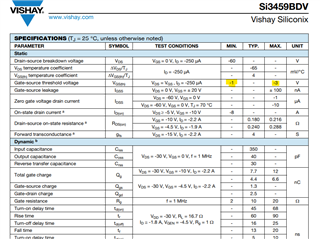
What I'm wondering is, there is a 2.5k ohm set resistor here, 0-5V input and 0-20mA output current. The supply source is 24 V, and when approximately 1.7 volt drop occurs, 22.3V/ (20*10^-3) = 1115 ohm, taking into account the rdson resistor and 15 ohm current limiting resistors, the maximum for a 0-20 mA configuration with this 24v supply is approximately 1.1 k ohm. We can use a resistor like . In the simulation, it is seen that the gate voltage drops to 7.34Volt. How was this value created? in datasheet External vgs ths value is min 1V  and max 3 Volts for this mosfet. In other words, when there is a difference of just over 3 volts between the mosfet and gate source, the gate opens completely.   Even if I apply gate 18 V externally, the mosfet turns on completely. How was 7.34v created?

digikey mosfet list link(click here)

Another question I have is about the selection of input capacitance and gate capacitance. I think as these values increase, the opening time of the MOSFET changes. Is there any effect other than this?

Best Regards 

Electronx

  • ±HI Electronx,

    The load resistance of 1.1kΩ is too high for a 24V supply XTR111 operation while requiring a 20mA output. When accounting for the series resistances, and required external transistor VSD voltage drop, this leaves much less than the 2V compliance required for the XTR111 operation.  T

    The XTR111 datasheet mentions the compliance range is limited to a voltage of 2V (+VVSP - 2V).  Then, in addition to this 2V compliance, we need to account for the external transistor VDS (drain to source) voltage drop, and any other series voltage drop in the current loop signal path:


    The circuit above has a 15 ohm series resistor at the source, and a 15 ohm resistor on the drain, adding an additional 0.6 voltage drop. Also, on a standard XTR111 current transmitter application, the length of the wire or cable will add series resistance. 

    Hence, the maximum voltage supported across the load resistor will need to be less than:

    VLOAD < 24V - (2V + VSD + (15Ω + 15Ω + Rseries)*ILOAD

    Therefore, the maximum voltage supported across the load resistor would be somewhere around ~21V, depending on the length of the wire (the series wire resistance), and the required VSD external transistor voltage drop to keep the circuit in linear operation.  The maximum load supported is less than <~1.050kΩ assuming a low wire resistance.

    The XTR111 will modulate the gate voltage until it reaches the target current.   The XTR111 circuit driving the gate is clamped, so it will not drive the gate more than 18V below the rail.  The Si3459BDV external transistor can tolerate a maximum of VSG voltage of ±20V without damage, therefore the FET will not be damaged by the XTR111. In addition, the external clamp circuit / ext. current limit circuit with the PNP bipolar transistor and 15Ω series resistor, described on page 13 of the datasheet, will clamp the VGS transistor voltage in case of a fast high current transient, when the load is inadvertently disconnected/connected during a fault.  

    The XTR111 was released to market on 2006, and unfortunately, there is no official released XTR111 TINA-TI or XTR111 PSPICE model.  The simulation shown above is only a simplified circuit to simulate the ideal transfer function of the XTR111. The simulation above does not encompass the input/output voltage and current limitations of the XTR111, DC errors, nor its frequency response.

    In the circuit above, there is no enough headroom for VSD drop to keep the circuit in linear operation, and the XTR111 would be out of linear range since it requires a 2V compliance from the VSP supply.  If you need to support a 1.1KΩ load with 20mA of output current, please increase the supply to VSP > ~+24.7V.

    Thank you and Best Regards,

    Luis 

  • Hi Electronx,

    The gate capacitance will primarily affect the rise time step response of the device.  Please see figures  31 and figure 32 for a 130pF capacitance on the VG pin.  A higher gate capacitance will slow down the step response, but will still work with the XTR111. The XTR111 is in primarily intended/used for relatively low frequency or DC precision applications.   If you require a faster response than the below, we could suggest other discrete solutions.

    Thank you and Regards,

    Luis