This thread has been locked.

If you have a related question, please click the "Ask a related question" button in the top right corner. The newly created question will be automatically linked to this question.

THS4532: Help for design review./confirmation.

Part Number: THS4532
Other Parts Discussed in Thread: ADC3641

Dear Friends

I am the first time to design a differential amp,  and seeking help to review/confirm my design.

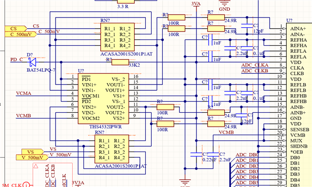
I have two analog signals: 0V to 2V, 0Hz to 2MHz,  to be fed to a differential input ADC. I don't have negative power, to get 0V signal, I use a 500mV reference (from an Op-amp) for the front-end instrument amplifier. therefore, the analog signals become 0.5V to 2.5V, I power the THS4532 with 3V, gain = 1 and Vcom = 1.5V(output from ADC).  Here is the schematic.

My questions /concerns to be confirmed are below.

1. though both analog and reference signals are from instrument amplifiers and Op-amp, the Inst-amp and Op-amp have different output impedances, I know closed-loop output impedances of Op-amp are very small, but they are indeed different, is it ok to ignore them?

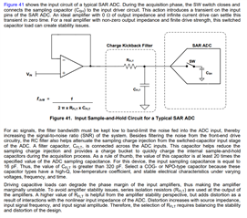
2. the ADC datasheet recommends an input (for ADC) filter of 25 ohm + 12pF cap, the 4532 also requires output resistor Ro,  I am not sure if I should combine Ro with 25 ohm together or separate them (as the schematic),  BTW, with ADC sample and hold cap = 4pF on each line, I am not sure if Ro = 100 ohm (as in schematic) is good or not.

3. When PDs are pulled down by a controller, is it ok to have 2V voltage fed to the input of 4532 since its absolute maximum Vid = 1V required in the datasheet?

4. Considering the analog signals are very wide dynamic and mostly DC nature,  any potential issue in the schematic design or any additional circuits may be suggested to optimize the design.

Thank you in advance

Tony

  • Hi Tony,

    Thanks for asking some really good questions.

    1. Yes, because the closed-loop output impedance is very small you do not need to worry about any impedance matching or any considerations for the output impedance difference.

    2. Can you clarify what ADC you are using? Typically, the charge kickback filter (filter at input of the ADC) has a capacitor value that is 20 times the value of sample and hold capacitor. Then the output resistor value can be determined from there. The TI Precision Labs videos for ADCs (found here) walk through this in the section SAR ADC input driver design under the math behind R-C component selection portion. If you were to use a 12pF capacitor in the charge kickback filter, you would need Ro to be around 200 ohms so that the FDA could operate with stability.

    3. When the device is powered down, the output will Vs-. Because you have Vs- at GND, a resistor divider is formed. This means that if the input signal is 2V, the voltage on Vin+ is 1V. And the voltage on Vin- would be 0.25V. Therefore, you would be within the abs max rating of Vid=1V. That being said, there would be less stress on the device if there was no input signal applied when the FDA is powered down.

    Thanks,

    Nick

  • Hi Nick

    Thank you for reply.

    The ADC we are using is LTC2295 from ADI. BTW, I couldn't find a counterpart from TI, 5-10MSPS, dual channel, 14-16 bit. 3-3.3V operates, either parallel or serial. Let me know if TI has the counterpart.

    I don't know how to select a cap for the kickback filter, what is an optimal cap value you may suggest for LTC2295?

    If Ro is required to be 200 Ohms by 4532, How about 25 Ohms of kickback filter? should I combine the two resistors into one resistor?  Or to separate them (as the schematic) and physically place them apart from each other during layout?

    Thank you

    Tony

  • Hi Tony,

    For your awareness, TI has a cross-reference search tool that allows you to search competitor parts and it will provide a list of TI comparable parts. The cross-reference search tool can be found here. TI has an ADC with similar function, ADC3641. 

    I am not familiar with the LTC2295 ADC so I can't comment on the optimal capacitor value for that device. As you mentioned, the datasheet uses 12pF and 25 ohms. I am not well versed with all ADC behavior; if you would like to know more on how to choose the capacitor value, I suggest opening a thread with on the ADC forum and they will have more knowledge on this topic.

    To answer your question: you can combine the two resistors into one. The kickback charge filter is a lowpass filter, so if you used two separate resistors a lowpass filter would still be formed with the series combination of the resistors and the capacitor. Having another resistor will add a little more noise to the system.

    Thanks,

    Nick

  • Hi Nick

    Thank you for the advice. it helps.

    I think 200 ohm with 12pF cap should be good for both chips.

    Best Regards

    Tony

  • Hi Tony,

    I would start with Ro set at 200 ohms. You can lower Ro if the distortion seen on the ADC is too large, however, there will be some increased peaking in the frequency response as you decrease Ro. If you have any other concerns, please feel free to reach out on this thread or a new thread.

    Thanks,

    Nick

  • Hi Nick

    Thank you for your support.

    Do you know what type of input signals may promote the potential distortion? DC or certain frequency signal? 

    I guess it might be a bit difficult for us to know or measure how much distortion the ADC is unless the distortion is very large.

    Best Regards

    Tony

  • Hi Tony,

    I believe the following snippet that discusses charge kickback filter design explains well the balancing between selecting the R and C component values. 

    To summarize, Ro is selected to avoid amplifier stability issues caused by driving a capacitive load. A larger Ro will add distortion as a result of interactions with the nonlinear input impedance of the ADC. The distortion will increase with source impedance, input signal frequency, and input signal amplitude.

    As you mentioned, this will not be especially noticeable if the distortion is low. So selecting Ro is balancing the amplifier stability and the distortion to meet your design constraints.

    I hope this clarifies your question. Please let me know if you have any other concerns.

    Thanks,

    Nick

  • Hi Nick

    That is well explanation.

    To our application, the interested band is 1-3MHz, as long as the distortion within this band is small, we will be good.

    if we use 200 Ohm + 12pF even including 4pF of S&H cap, the cutoff frequency is far higher than 3Mhz, we should be safe, right?

    Thank you

    Tony

  • Hi Tony,

    Using a 200 ohm resistor and 12pF capacitor will create a low pass filter with a cutoff frequency much higher than 3MHz so you will not impact the signal in the band of interest. However, because the cutoff frequency is much higher than the band of interest, you are susceptible to distortion in the ADC coming from wideband and signal harmonics that may appear. Because the ADC is not a TI part, I am unable to qualify what distortion you may see from that device. 

    You can use the TI Precision Labs videos for ADCs that I linked in a previous reply to help calculate R and C component values if the distortion is still a concern. Another option is to start with Ro of 200 ohms and if the distortion is too large, you can decrease the value. However, caution should be taken as decreasing Ro too far could cause instability of the amplifier.

    Thanks,

    Nick

  • Hi Nick

    Thank you for the reminder.

    To take care of wideband and harmonic distortion, we can filter the data with digital processing after ADC.

    The filter recommendation from ADI is with an even higher cutoff frequency, maybe the ADC is good enough in terms of wideband distortion.

    Thanks

    Tony

  • Hi Tony,

    It seems like all your questions are now resolved so I will close this thread. If you have any further questions you can reply to this thread or create a new thread.

    Thanks,

    Nick

  • Hi Nick

    Thank you for your great support.

    Regards

    Tony

  • Hi Tony,

    I'm glad I could provide assistance.

    Thanks,

    Nick