This thread has been locked.

If you have a related question, please click the "Ask a related question" button in the top right corner. The newly created question will be automatically linked to this question.

INA333: Design issue for INA333

Part Number: INA333
Other Parts Discussed in Thread: OPA333, TPS22925

Hi,

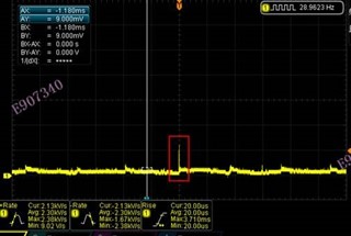
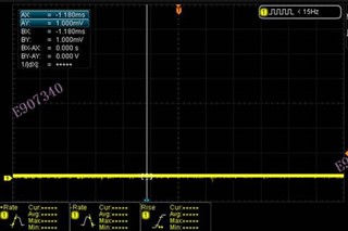
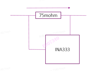
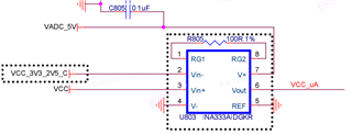
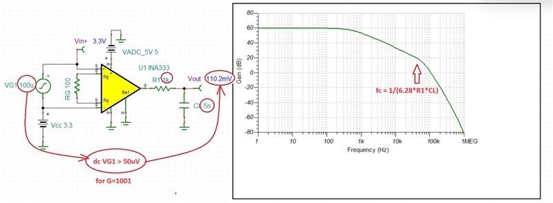
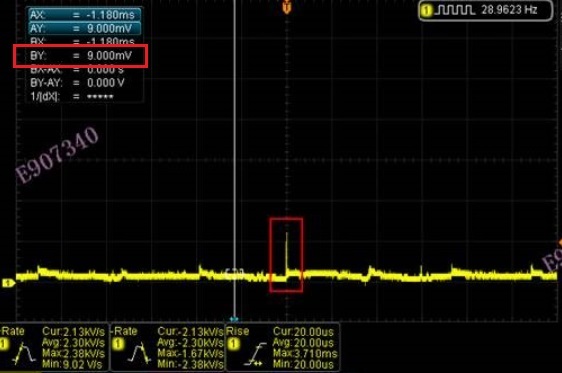
We use the INA333 for the signal amplification, and now, it has the pulse signal after the INA333, the amplitude is about hundreds UA(GAIN=1000), 

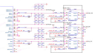
Please refer to below schematic and provide your commend that there are any error, thanks.

  • Hi Zhang,

    You refer to INA333 but your top schematic only shows TPS22925 while the bottom picture shows floating circuit with no reference to any supply voltage. Thus, you provide no actual details to analyze the circuit.  Having said that, OPA333 operational amplifier uses an auto-calibration technique with a time-continuous 350-kHz operational amplifier in the signal path. This amplifier is zero-corrected every 8 μs (fc=125kHz) using a proprietary technique, which in the high gain like 1,000 may show at the output as a glitch - for this reason, in order to remove these output spikes you may have to add a low-pass RC filter at the INA333 output with fc<40kHz.

  • Hi Marek,

    Thanks for your kindly comment.

    The below is the schematci diagram for INA333, please also provide the range of the RC, that we can modify design base on your suggestion, thanks.

  • Hi Zhang,

    The output low-pass filter components should be calculated using a simple fc=1/(6.28*R1*CL) equation - see example below.

    However, looking closer at your scope seems that the output is at negative rail (9mV) above ground) that is NOT allowed - see below.

    Your single supply setup with Vref grounded requires a minimum +50uVdc differential input voltage for the output to be within its linear range of 50mV above negative rail - see datasheet table below.  Otherwise, the output will be trioded (operating in a non-linear region), which would results in the output glitches you complain about because this condition leads to a large offset voltage that INA333 would futilely attempt to correct generating output glitches you see.

    INA333 Zhang circuit.TSC