Because of the Thanksgiving holiday in the U.S., TI E2E™ design support forum responses may be delayed from November 25 through December 2. Thank you for your patience.

This thread has been locked.

If you have a related question, please click the "Ask a related question" button in the top right corner. The newly created question will be automatically linked to this question.

OPA858: Photodiode Pulsed Current

Part Number: OPA858
Other Parts Discussed in Thread: OPA855, OPA856, OPA615, OPA860

Hi,

I need support about a new design.

We have a photodiode integrated in a laser diode driven by a pulse train (40mA peak, 5Hz-50kHz PRF, Duration 15ns).

We want to design a conditioning circuit to convert the pulsed current in the photodiode in an average or peak voltage signal to be measured by an ADC of a microcontroller so to have a sort of average or peak optical power measurement.

We want to use a TIA (for example OPA858) with an integrator circuit or something like that. Is it possible? Do you have a good solution?

Can you please give us support in the design?

Thanks in advance.

Best Ragards

  • Hi Antonio,

    I would be happy to provide support for your new design. I have some confusion on what your application and needs are and I am hoping you can provide some clarifications on a few things:

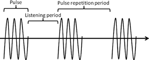
    1. When you describe your pulse train input, are you referring to a waveform like shown below? For the pulse duration of 15ns, is the frequency or amplitude of the pulse signal changing? And does the pulse signal have a sine waveform or another waveform? I assume that the listening period would change depending on the PRF and that the pulse duration is set at 15ns (i.e. if the PRF is 5Hz, there would be 5 pulses of 15ns over a 1s time interval).


    2. Do you have a specific microcontroller/ADC picked out?

    3. In transimpedance amplifier applications, the output voltage waveform of the amplifier will match the input current waveform (with the obvious transformation from current to voltage through the feedback resistor). An integrator circuit typically take a voltage input waveform an performs an integration (i.e. an input square wave will have an output triangle wave or an input sine wave will have an output cosine wave). Neither circuit takes an average of the input signal. Based on this, can you share what your application? And is your goal to convert the input current signal to an output voltage signal and then the microcontroller will handle all processing of the signal?

    Thanks,

    Nick

  • Hi Nick,

    1. The pulse is a simple 15ns rectangular pulse with no sine carrier, PRF is 5Hz---50kHz so 5Hz means 5 pulses in 1s ------- 50kHz 50.000 pulses in 1s. Pulse Ipeak of laser diode is 40mA (---> 30mW peak optical power of pulse), Pulse Ipd of photodiode is 12uA (corresponding to 40mA). So there is no modulation. It is on/off signal, Ion=Ipeak = 40mA (12uA) / Ioff=Low Current little below the threashold current of laser diode to have a faster turn on.

    2. STM32 family Microcontroller, ADC could be also external if it is necessary for performance.

    3. We want to measure the average or peak optical power emitted by laser diode using the integrated photodiode. Since the pulses are very narrow I think that the best solution is to bring out the information by accumulating n current pulses (using as first stage a TIA to convert the current pulses in voltage pulses). We need this information from photodiode both for the calibration that would be done before firing the pulse train with a long pulse in order to be sure that the optical output power is what we expect, but we would also like to use this information for a possible safety shutdown in case a power exceeding a certain maximum permitted value is coming out. So crucial is to have a sort of information about what optical power is coming out, for initial calibration (it could be 1 long pulse in this case), for real time readout and for safety.

    I think that it is typical application of pulsed laser diode to take the pulsed signal from photodiode to do measurement. it would be nice if there was an already existing solution ready to be adapted to our purpose.

    Let me know if it is all clear. I am available for further clarifications.

    Thank you for your support.


  • Hi Antonio,

    Thank you for the clarifications. In order to design the TIA stage, a few things need to be considered:

    1. What gain are you looking to achieve (based on what the ADC input range is)? For photodiode current pulses of 12uA, a gain of 100kohm would result in an output voltage swing of 1.2V for example

    2. What are your rise/fall time and settling time requirements?

    3. Will you have a filtering stage between the TIA stage and the ADC? Can you share what the capacitive load of the ADC is?

    Thanks,

    Nick

  • Hi Nick,

    1. 1.2V could be good, Just a mistake, I said 12uA for photodiode, instead it is 72uA. So resistor has to be changed.

    2. Rise/fall time and settling time requirements about the pulse you mean?

    3. Do you think that it is possible to measure the 15ns pulse train directly with an ADC? If necessary, we can have a filter stage. Anyway the ADC could be external, so you can suggest one.

  • Hi Antonio,

    1. Thank you for correcting this. I would now consider a possible gain of 20kohm which would produce an output voltage swing of 1.44V. Again, this can be tuned to match the full scale range of the ADC of your microcontroller or of the external ADC if that is what you choose.

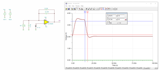
    2. The output voltage pulse created from the current-to-voltage conversion will take a pulse waveform shape, as you would expect. However, because the amplifier has a limited bandwidth, it will not be able to instantaneously change the output voltage and so there is an inherent rise and fall time. This can be calculated by: rise time = 0.35/closed loop bandwidth. The closed loop bandwidth varies based on the total input capacitance, feedback resistor, feedback capacitance, and op amp GBWP. Here is an example using the OPA855. Here the rise/fall time is about 3ns:

    However, this is assuming a photodiode capacitance of 5pF and very tight specifications for the feedback capacitor. If it is not necessary to have this small of rise/fall time, some of the specifications can be relaxed. 

    3. I can look into what ADCs might fit this application so I will get back to you on this. Can you share the specifications of the internal ADC of the microcontroller as well?

    Thanks,

    Nick

  • Hi Nick,

    in the laser diode datasheet there is no information about photodiode capacitance.

    The microcontroller will be a nucleo board STM32F439ZIT6 in this prototype session.

    Best Regards

  • A TIA design cannot really be done without the diode capacitance, the lower the better. You need to request that from the manufacturer. 

    Also, most high speed photodetectors are reverse biased to reduce their souce C, so you really you need the plot of C vs reverse bias to proceed. 

  • Hi Nick,

    another information.... the photodiode catode is connected to positive supply. So I think we need also an inverter after TIA.

  • Hi Michael,

    thanks for your support.

    We are going to request specific information from manufacturer as soon as possible..

    Best Regards.

  • Hi Antonio, 

    As Michael mentioned, the TIA design can not be tuned without knowing the photodiode capacitance and this is dependent on how you are biasing the photodiode as well. When you are able to find this information from the manufacturer, please let me know and I can help tune the design.

    Have you determined if there is an acceptable rise/fall time requirement for your application?

    And thanks for providing information about the microcontroller. I will look into the specifications of the ADC.

    Thanks,

    Nick

  • and, if you have current going into the TIA V- node, you could bias the V+ op amp input at the desired output and ltet it go down from there. The eventual peak and averaging circuits would work easier with a 0 to some peak voltage going up so an inverter would be useful but not necessary. 

  • Hi Nick,

    ok I will provide you with information about the photodiode as soon as possible.

    The current pulses passing through the laser diode will have a duration of approximately 15ns and a peak of 40mA (30mW), the corresponding peak current in the photodiode should be approximately 72uA based on what is reported in the manufacturer's datasheet. I don't know now how the current waveform output from the photodiode will be deformed, but I still imagine that it will be a very narrow pulse with trise/tfall of the order of a few ns. Keep in mind that the objective is on the one hand to do an offline calibration with a long pulse of current of the necessary amplitude (40mA) to release the desired power (30mW) and re-read the amplitude of the photodiode current to know which optical power is actually coming out, and on the other hand during the sending of the pulse train with PRF programmable between 5Hz and 50kHz being able to collect a valid information from the photodiode that can be connected to an average or peak power of the pulse train to be used for measurement of the power and also compare it for safety reasons with some threshold to disable the emission in case of exceeding the permitted power limit.

    Thanks

  • Hi Michael,

    you are right. If we use Vbias (for example 1.8V as suggested by Nick) it is not necessary an inverter stage.

    At the end we have to understand what is the best solution to capture this train of impulses from photodiode and come up with a sort of voltage value representative of the power that the laser diode is emitting and then measuring it with an ADC.... or measuring every single pulse with an ADC but I don't know if it is possible.

    Thanks

  • Hi Antonio,

    Thank you for this clarification. As mentioned previously, I will help tune the component values when you get an answer from the photodiode manufacturer.

    Thanks,

    Nick

  • Hi Nick,

    we requested the information but unfortunately the manufacturer does not have it. So what we can do is to assume some junction capacitance and shunt resistance to proceed with the design. Then when we have the laser diode we will try to do some tests to characterize the device.
    For now, maybe let's try to hypothesize Rshunt 1G and Cj 5p, then we will make adjustments to the design, also because it is a prototype.

    Let me know.

    Thanks.

  • Hi Antonio,

    Based on this information, you can use the design that I previously created using the OPA855. You will be able to achieve a rise/fall time of around 3-5ns as I show in simulation if the photodiode capacitance is 5pF. It sounds like with the photodiode that you are using, the photodiode will be sourcing current into the amplifier so the output voltage will be inverted from what I have shown. With this, you may need to adjust the reference voltage on V+ so that the lower output swing limit does not cause clipping.

    If you find that the photodiode capacitance is different from this value, you can use the TIA calculator that I have linked above in order to determine a new feedback capacitor value for your feedback resistor value and closed loop bandwidth.

    Thanks,

    Nick

  • Hi Nick,

    ok thanks for information. Yes, the photodiode will be sourcing current into the amplifier so the output is negative but eventually we could use an inverter.

    Can you suggest a good solution for the integration of this ns pulses?

    Best Regards.

  • Hi Antonio,

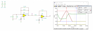
    Here is a possible circuit configuration with the OPA855 as your TIA stage and the OPA856 as an integrator stage. The integrator stage also inverts the output of the TIA stage. You can use the integrator circuit design notes (found here) to help make any adjustments to the circuit you may need to fit your application.

    OPA855_TIA_OPA856_Integrator_E2E.TSC

    Thanks,

    Nick

  • Hi Nick,

    I took a look at the proposed solution. What we want to get is a measurement of optical power, so we need to somehow measure what comes out of the integrator. We have a uC available that could interface with an external ADC and I see that the input that comes out of the integrator is very narrow and perhaps difficult to acquire. Perhaps we could bring out the peak of these pulses in order to have an easily measurable continuous signal. Furthermore we also need to measure the peak of the pulses coming out of the OPA855 and the presence of the 3V pedestal makes this more complicated. Perhaps it would be more appropriate to have a dual power supply in order to have a negative impulse from OPA855 followed by an inverter and send it to a precision peak detector. It must be kept in mind that both the integrator and the peak detector must work well in the PRF range 5Hz-50kHz. I also took a look at OPA615 and OPA860 that could be useful for our scope.

    I hope you can help us.

  • Hi Antonio,

    Yes, you can certainly add an inverter stage that would go to a peak detector for the uC to read the current to voltage conversion of the TIA stage. As you suggested the OPA615 has a very useful configuration for a peak detector. This is discussed further in this E2E thread: https://e2e.ti.com/support/amplifiers-group/amplifiers/f/amplifiers-forum/167314/super-high-speed-peak-detector-needed 

    Also, I do not have a vast knowledge of what the best options for ADCs are. My recommendation is to open an E2E thread for the ADC team who will be able to assist further in selecting the proper ADC for your application.

    Thanks,

    Nick

  • Hi Nick,

    attached you can find a classic circuit for peak detection but it doesn't seem to work. Why?

    Can you check if there is something wrong?

    OPA855_TIA_OPA856_PeakDetector_E2E.TSC

    Best Regards.

  • Hi Antonio,

    I am looking into why the circuit is behaving as it is in your simulation schematic. I look to have more answers by the beginning of next week.

    Thanks,

    Nick

  • Hi Nick,

    do you have any news for me?

  • Hi Antonio,

    I apologize for not getting back to you sooner. I was investigating the circuit that you sent to me because the changes you made seem to make it unstable. However, I have been trying to simulate using single supply like I originally recommended and I believe the peak detection circuit is working all though the held peak value decays after some time. I was working on looking into how to adjust this, but I can share what I have so far.

    OPA855_TIA_OPA856_Integrator_and_Peak_Detection_E2E.TSC

    Thanks,

    Nick