This thread has been locked.

If you have a related question, please click the "Ask a related question" button in the top right corner. The newly created question will be automatically linked to this question.

TLV271: TINA simulation results conflict with reality

Part Number: TLV271
Other Parts Discussed in Thread: TLV9151

Hi,

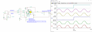
I have a TINA simulation of the TLV271 in a differential amplifier configuration. The simulation worked well however the actual circuit does not. It appears that the simulation generates invalid output when the input pins are driven below the negative supply rail. TINA file attached.

diff amp driven below neg supply rail.TSC

  • Hi David, 

    Could you clarify what you are trying to do with the input signals? What is the magnitude and frequency for each input? I'm not quite sure I understand from the TINA simulation you provided. Also if you have actual circuit results (oscilloscope images of inputs, outputs, etc), that would be very helpful. 

    Please let me know if you have any questions.
    Thank you!

    Best Regards,
    Ashley

  • Hi Ashley,

     The circuit is designed to measure a 12V signal (VG1) differentially in the presence of a high common mode voltage (VG2).   If you run the transient simulation VG2 varies from +60V to -60V while the input signal transitions from 0V to 12V. The simulation results look just fine however if you watch VM4 you can see that the voltage at the input pins of the op-Amp goes below the negative rail, which in this design is ground. 

    Whenever the input pin is at or below ground the output collapses. Actual circuit measurements with 0V, +/- 30V,+/- 45V, and +/- 60V offset applied.

    You can see that positive offset works as expected, as does -30V, however when -45V and -60V are applied the output is invalid. The TINA SPICE model should have limited the design when the input pins started to fall below the negative rail.

  • Hey David,

    I can shed a little more light on this. The TLV271 is based on an older macromodel architecture which had some limitations. Namely among these is that the inputs are not diode clamped to the rails. You can see that the input is able to go beyond the abs max datasheet rating.

    The older models require a little more care, as they may give some nonsensical answers, or they can be worked around by manually adding the diodes to V+ and V-. 4784.diff amp driven below neg supply rail.TSC

    Unfortunately we are not slated to update this model as we are focusing on new developments.

    In our more updated devices, the inputs are properly clamped.

    Best,
    Jerry

  • Jerry,

    Thanks for the explanation. two comments on that, I understand that you have no plans to update older models, but then that warning should be on the download page for each part that the model applies to. Also thanks for adding the diodes, the inputs look correct, but the output generated and shown on VM2 still does not match the actual circuit, at the point the inputs clamp the output should collapse

    Dave

     What TINA TI part would you recommend I use the model for that would be more realistic? IE newer model op-amp in same pkg?

  • Hey David,

    I see that this part is not specified as resistant to phase reversal, which may be what you are seeing when you exceed the VCM below the negative rail. Generally phase reversal is not a simulated behavior, even in our latest models.

    However, the TLV9151 is a great newer equivalent with our updated model architecture. It's rail to rail in/out and you get an extra 1.5MHz of typical bandwidth out of it for pretty much the same typical Iq (10uA more).

    Best,
    Jerry