This thread has been locked.

If you have a related question, please click the "Ask a related question" button in the top right corner. The newly created question will be automatically linked to this question.

INA296A: Floating noise much higher than spec

Part Number: INA296A

Hi,

I trying to use the INA296A5QDDFRQ1 in this configuration:
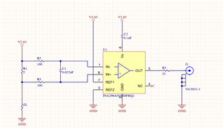


where R1 is the current sensing resistor. However, when I try to get a baseline of the offset voltage and input bias current with no load or power,
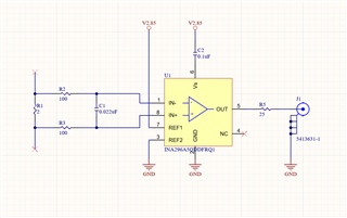


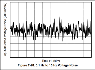
the output voltage is much noisier than what is reported in the spec:


What can I do to reduce the noise?

  • Hello Will,

    Due to the fact that our input stage is not high impedance you will need to have a current path at the input (35µA typical at each input pin).  Leaving it floating is not an option for calibrating the offset.  Also due to this input bias current I would remove the R2 and R3 or make it lower if possible.  If the output is only driving a small capacitance ex:  scope probe then you are fine.  If you are driving a larger capacitance above 1nF please increase R5 to abut 200Ω.  

    You could connect the inputs to ground or the 2.85V supply.  Ideally you would use the voltage you would use it at but the very small difference and the good CMRR you may be ok.

    Regards,

    Javier


  • Hi, thanks for the response.


    Regarding the noise, it is present with(right) and without(left) a DC bias path.

    Regarding R2 and R3, the noise was present without them. 100 Ohms would not remove the DC bias path. It is only a 3.5mV drop.

    We are outputting to a scope probe so there is not a large output capacitance.


    Thanks,

    Will Larsen

  • Hello Will,

    I am sorry you are comparing the low bandwidth noise with full bandwidth.  This plot you show is for low frequency only with a filter to limit the bandwidth.  For full bandwidth the value for INA296A5 we use the 28nV/√Hz.  The two videos below go over the calculations I have

    https://www.ti.com/video/4078827152001

    https://www.ti.com/video/4078839879001

    For INA296 full bandwidth of 1.1MHz 

    Assuming 1st order of the INA296 use 1.57 correction factor.  This is an assumption and used for easy calculation.  This device is more complicated but good estimate.

    BW= 1.1MHz *1.57

    Noise 28 nV/√Hz

    Gain =200

    RMS noise = 28 nV/√Hz * √(1.1MHz *1.57) = 36.8µV RMS input referred.

    Input to output multiply by gain 200.  Output referred 36.8µV* 200 = 7.36mV

    RMS to Peak to Peak = 7.36*6 = 44mV

  • Hi Javier,

    Thank you for the noise explanation. This makes sense. I didn't realize that plot was low BW.

    In another reply, you said that we may increase the output resistance to 200Ω if the output capacitance is > 1nF(the max capacitive load). Can you tell me how you calculated this value? Is it based on the corner frequency derived from the total output resistance of the amp? Op Amps Driving Capacitive Loads | Analog Devices. In this article, the "Out-of-loop compensation" section describes this calculation. I don't believe the datasheet contains the output resistance. Can you provide this to me?

    Thanks,

    Will

  • Will,

    I normally just throw the rule of thumb out there.  For more detail you can see our application notes or run simulations to verify your stability as the output impedance is modeled.  

    https://www.ti.com/lit/an/sboa443/sboa443.pdf

    https://www.ti.com/lit/an/slya029/slya029.pdf

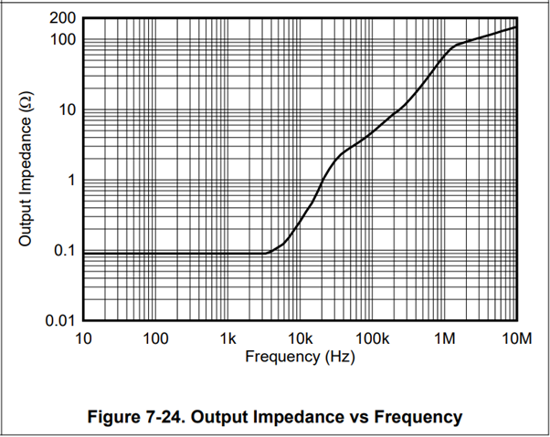
    My rule of thumb is just have the resistor larger than the output impedance of the device if available.  For this device it is 200Ω.   The output impedance is in the datasheet.  Screen shot below attached below.

    Regards,

    Javier