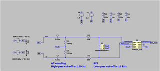
Hi,
In my design I used INA 351 for instrumentation amplification in EEG sensor. I simulated my design and everything was working properly, but on PCB I couldn't get logical output. In the datasheet of the INA351, it is written that
" Differential input voltages greater than 0.5 V applied continuously can result in a shift to the input offset voltage above the maximum specification of this parameter. The magnitude of this effect increases as the ambient operating temperature rises."
In my design Vref voltage is also given to the system as an offset between R1 and R2, I couldn't be sure datasheet mention about the difference between two input signal or the offset voltage at inputs.
If you could help me I would be too happy.

-
Ask a related question
What is a related question?A related question is a question created from another question. When the related question is created, it will be automatically linked to the original question.

