This thread has been locked.

If you have a related question, please click the "Ask a related question" button in the top right corner. The newly created question will be automatically linked to this question.

INA125: Difference between part markings

Part Number: INA125

Hi All

Can someone help me to understand the difference between the following part numbers?

INA125U36AFF3K

INA125U36AFF5K

INA125U36AFF9K

I am trying to understand if this would affect the results I am getting when using these parts in my circuit of whether it is something else. Your help in this matter would be greatly appreciated Slight smile

  • Hey Graham, 

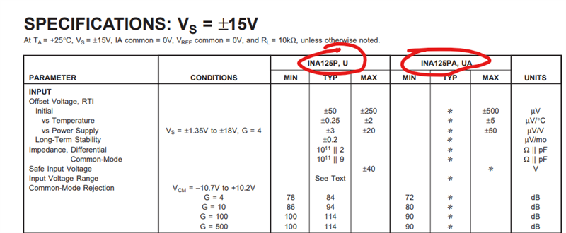
    Can you point me to where you are seeing 36AFF3K, 36AFF5K, 36AFF9K attached to INA125U? There is a grade out with different specifications in the datasheet that can certainly result in different performance.

    The orderable devices are listed below:

    Best Regards,

    Chris Featherstone

  • Hi Chris

    The number I am referring to is the number that is printed on the body of the component. Maybe the number is just some internal information like a batch code or something. It was just something that I wanted to rule out. 

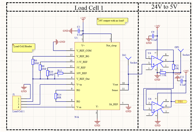
    What I am seeing is a difference in Voltage for the V- Pin and the V+ Pin across two components of 0.070mV. Issue is this is then going through a further two amplifiers and by that stage the differences are very different. See below

    Just trying to work out if this difference is normal across multiple chips or is there something wrong?

  • Sorry the MPN for U4 and U6 is LTC2057HS8#PBF from Analog Devices.

  • Hey Graham, 

    Based on my understanding of the issue the 70 uV you are observing fits in the expected offset distribution. The input offset voltage can range from -250 uV to +250 uV or -500 uV to + 500 uV depending on the grade out. On the INA15P, U the typical input referred offset voltage is 50 uV. 

    Best Regards, 

    Chris Featherstone

  • Sorry Chris

    just realising here that I used the wrong units. It was a difference of 70 mV not uV. 

  • Hey Graham, 

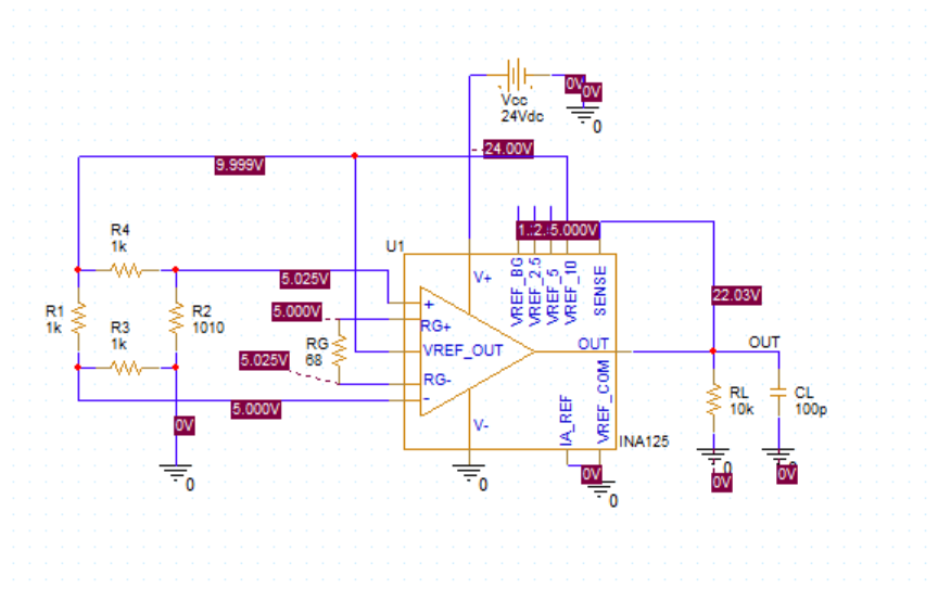
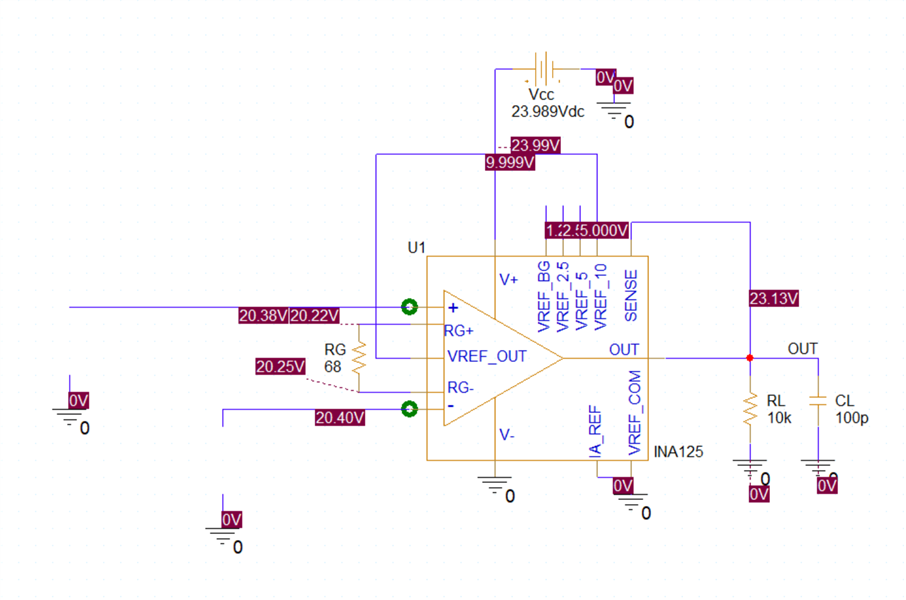
    Is the 70 mV difference output referred or input referred? Your gain is 888.4 V/V. If this difference is output referred we can divide by the gain and see that the input offset is about 78.8 uV. If this is not the case then we need to investigate further in which case I have provided an example below in simulation. We would need to know the node voltages on your circuit in order to determine if everything is within the linear operating range. Can you also provide us what the equivalent bridge sensor looks like for simulation purposes? I have given an example below. I would want to alter my simulation such that I am matching your conditions. Providing the node voltages as shown below will tell us a lot. 

    Best Regards, 

    Chris Featherstone

  • Graham, 

    To add to my last post, it would be helpful to isolate the issue and make the node voltage measurements without the op amps on the output of the INA so we can determine if everything with the INA is operating as we would expect. 

    Best Regards, 

    Chris Featherstone

  • HI Chris

    Please see below a table of the voltage readings I am getting at each pin on the chip.

    U1
      Function PCB 1 PCB 2 Difference (V)
    1 V+ 23.989 23.987 -0.002
    2 SLEEP 23.989 23.987 -0.002
    3 V- 0.000 0.000 0.000
    4 VrefOUT 9.998 9.989 -0.009
    5 IA Ref 0.000 0.000 0.000
    6 Vin+ 0.160 0.230 0.070
    7 Vin- 0.160 0.230 0.070
    8 Rg (Gain) 20.239 20.233 -0.006
    9 Rg (Gain) 20.265 20.260 -0.005
    10 Vout 23.203 23.197 -0.006
    11 Sense 23.203 23.197 -0.006
    12 Vref COM 0.000 0.000 0.000
    13 Vref BG 1.230 1.229 -0.001
    14 Vref 2.5 2.492 2.493 0.001
    15 Vref 5 4.989 4.991 0.002
    16 Vref 10 9.990 9.991 0.001

    Hopefully this is the information that you need.

    Best Regards

    Graham

  • Hey Graham, 

    What is connected to the inputs during these measurements? Are the inputs floating? If so the amplifiers are railed out in which case the device is not operating within the linear operating range? Can you show me how the input is connected similar to what I have shown in my schematic above? Based on what I am seeing the outputs are in the supply rails indicating that there is nothing connected to the inputs. 

    Best Regards, 

    Chris Featherstone

  • Hi Chris

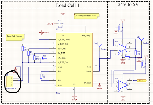
    So you are correct in saying that there is nothing currently attached to the inputs. It would normally be a load cell. The load cell we are using is the Flintec PA1. The reason for not having a load cell attached for our measurements is because we are just trying to verify the PCB with no inputs or outputs connected. I have highlighted in the schematic below where we normally connect our Load cell in the circuit.

  • Hey Graham, 

    Yes if you leave the inputs floating then the internal amplifiers have no direction as to where to go. The output will attempt to correct for input error and will rail out as shown below. You would want to tie the inputs to a known voltage level such that the inputs are not floating. 

    Best Regards,

    Chris Featherstone