This thread has been locked.

If you have a related question, please click the "Ask a related question" button in the top right corner. The newly created question will be automatically linked to this question.

THS4151: Calculation formula for offset adjustment circuit of THS4151ID

Guru 10090 points
Part Number: THS4151

Hi,

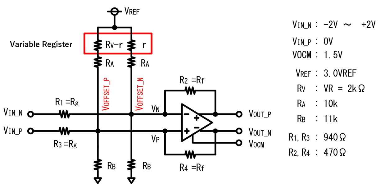
Is the calculation formula for the THS4151ID offset adjustment circuit correct?
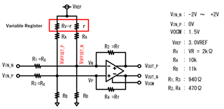
■Output common mode voltage
VOCM = (VOUT_P - VOUT_N) / 2

■Output differential voltage
VOD = VOUT_P - VOUT_N

If R1 = R3 = Rg ,R2 = R4 = Rf...

(Output voltage (input voltage + offset voltage) × Rf / Rg)
■Positive output voltage
VOUT_P = ( VIN_P + VOFFSET_P) × Rf / Rg
■Negative output voltage
VOUT_N= ( VIN_N + VOFFSET_N) × Rf / Rg

We would appreciate it if you could check it out.

Thanks,

Conor

  • Hi Conor,

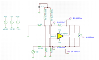
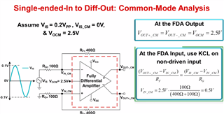
     I was able to recreate your circuit in a TINA and it looks like it would work as a way to tune the offsets produced by the device; as an example, here is the same circuit with a 1V reference. You can see as you tune the resistors which will give you different "offset" voltage; however, this is also affected by the VOCM pin which is described in the below slide. Therefore, there is more at play with the way these values are calculated. The slide is from our TI precision lab videos if you interested in the analysis at this link.    


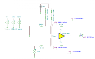
      I found it easier to tune the voltages by removing the Rb resistors as shown below: 

    Best Regards,

    Ignacio

  • Hi Ignacio,

    Thank you for the information on the simulation tool. I checked the following materials, but I wasn't sure if the formulas for VOUT_P and VOUT_N that I wrote in my first post were correct.
    https://www.ti.com/lit/an/slyt157/slyt157.pdf

    If I derive it from a calculation formula rather than a simulation, is the calculation method I described correct? If there is a difference, please let me know.

    Thanks,

    Conor

  • Hi Conor,

    The calculations in the article are derived specifically for the configuration highlighted in Figure 1. Adding the additional components changed the functionality of this circuit which would mean the derivation in the article will not apply to this circuit. The likely way to try to create a transfer function for this circuit is applying superposition. You can then use simulation results to confirm if the derivation is accurate. 

    Best Regards,

    Ignacio

  • Hi Ignacio,

    I'll try running the simulation this Friday. Also, could you please tell me the formula for introducing VOUT_P and VOUT_N on the circuit below? Are my VOUT_P and VOUT_N correct?

    Thanks,

    Conor

  • Hi Conor, 

    I assume that ultimately what you are trying to do here is provide a DC differential output offset to the circuit. The circuit diagram you provided would achieve that to some degree, but it is very hard to solve the circuit due to the unbalanced impedances caused by the input network. 

    Typically to achieve this type of function you would use a circuit like below where Ra1+Rb1 = Ra2+Rb2 (Ignore the three ideal op-amps, that is just a way to model an ideal differential amplifier).

    In this case, when Vin = 0, the differential output offset will be Vout = Vref * Rf * (1/Ra2 - 1/Ra1). You can then just choose resistors appropriately to set your offset. 

    Regards, 

    Jacob