This thread has been locked.

If you have a related question, please click the "Ask a related question" button in the top right corner. The newly created question will be automatically linked to this question.

OPA2196: Output circuit configuration information

Part Number: OPA2196
Other Parts Discussed in Thread: TLV9002, OPA2322

Hello,

I would like to confirm output configuration of OPA2196.
I'm looking for device which can reduce crossover distortion.
In general, TI release "zero-crossover" product so I should choose device from these lineup.
However, current "zero-crossover" devices only support up 5.5V as supply voltage.
I would like to use 10V(+/-5V), so need to confirm from another approch.

Then, I found e-trim product. it seems this tech reduces input offset distortion. So we can expect decreasing crossover distortion comparing to general device.
However, I'm not sure effect of output from viewpoint of crossover distortion. Do you have any information which arch is used or you also have tech for output stage from viewpoint of crossover distortion ?

BR,

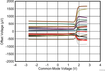
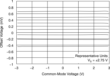
  • TI's "zero crossover" feature indicates that the opamp uses a charge pump so that a single transistor pair can cover the entire input voltage range. On rail-to-rail opamps without this feature, the crossover between the N-channel/P-channel (or NPN/PNP) input pairs is visible in the offset vs. common-mode voltage graph; for example, below are shown TLV9002 and OPA2322:

    This feature is used only for low-voltage rail-to-rail opamps because at larger voltages, it is easier to avoid the bad part of the input voltage range.

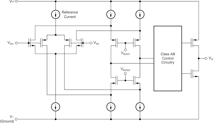
    Regarding the output crossover distortion, there is no feature that would explicitly indicate that an opamp is designed to avoid this. However, modern opamps actually do this by using class AB output drivers:

    The only way to search for low output crossover distortion is to look for opamps with a high CMRR (this value covers both input and output distortion; check that the value is tested over the input voltage range that you care about).
    (For how the OPA2196 behaves in the input transition region, see section 7.3.6 of the datasheet. Note that the CMRR in section 6.7 is specified for multiple ranges.)

  • Hello,

    Thank you for your explanation.
     >However, modern opamps actually do this by using class AB output drivers:
    Yes, I also have same idea whether device can reduce output crossover distortion.
    (Some opamp have combination A output driver with C output driver. Such opamp will cause large output crossover distortion.)
    I would like to know whether there is any way to recognize output driver type.
    However, from your reply I think that it is difficult to recogize output driver except supplier disclose configuration type in datasheet. Or as you said, is it possible to recognize output type from CMRR spec ?

     BR,

  • BR,

    There are really two phenomena that are called "crossover distortion".  One form of crossover distortion is sometimes called "input crossover distortion".  This type of distortion is related to a rail-to-rail common mode input that uses two input stages.  This Op Amp Input and Output Swing Limitations document describes this limitation in detail.  Note that this is related to common mode input swing so the issue is only noticed in non-inverting configurations where the input signal range approaches the power supply rails.  The other form of crossover distortion is sometimes called "output crossover distortion.  Output Stage Distortion is a good video on the subject of output stage distortion (including output crossover).  In general, I think that output crossover concerns are more significant in power op amps.  Small Signal Amps and Power Op Amp Crossover Distortion.pdf is a presentation that covers power op amps and crossover distortion.  If distention is your key concern, I would look at the various THD+N plots to see if the amplifier meets your requirements and not focus on output crossover distortion.  However, as Clemens pointed out, you may want to pay attention to input crossover distortion for this device and either limit the input signal common mode range or use an inverting configuration to minimize distortion.  

    Best regards,

    Art

  • Hello,

    Thank you for your explanation.
    I understood which point is important to check output crossover distortion.
    I will close this thread.

    BR,