This thread has been locked.

If you have a related question, please click the "Ask a related question" button in the top right corner. The newly created question will be automatically linked to this question.

OPA847: Capacitance calculation to remove oscillations at low gain regime (transimpedance configuration)

Part Number: OPA847
Other Parts Discussed in Thread: OPA856

Hello,

We have a PCB circuit with the OPA847 amplifier in transimpedance configuration. We wish to work in a low gain regime with a resistance in the feedback loop of 220 Ohm. The circuit has been tested with feedback resistance values from 1kOhm to several kOhm without any problems (there were no capacitor in the feedback loop and the bandwidth was around 50 MHz). When we set a resistance lower than kOhm, we see oscillations with amplitudes in the hundreds of mV. With this resistance value of 220Ohm fixed (we need a low gain), we want to find the value of the capacitance to be shunted in the feedback loop. Taking into account the equations in the tutorial section, we found that the capacitance value should be less than a hundred nF. We've tested with a different values of capacitance between few pF to hundred of nF, but the problem persists. Our only constraint is to have a bandwidth of at least 20/30 MHz and a feedback resistor of 220Ohm. How can we determine the value of the capacitor?

We have a related question. Is it possible to buy an evaluation PCB designed for a transimpedance configuration with the OPA847 amp, as well as a place for a photodiode?

Thank you very much,

  • Hi Adrien,

    We have a transimpedance amplifier (TIA) calculator that can be found on our high-speed amplifier FAQ page (here) along with some other great information about TIA configurations.

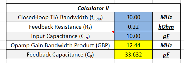
    Using Calculator II, you can plug in the closed-loop bandwidth, feedback resistance, and input capacitance to determine what feedback capacitance you need and if the device you are using has a large enough GBP. Note the input capacitance is the capacitance of the photodiode + 3.7pF which is equal to the input differential and common-mode capacitance of the OPA847.

    I would be happy to help support your design. I can help find the right passive component values and provide a simulation file if you are able to provide a few more details:

    1. What is the photodiode capacitance?

    2. What is the magnitude and frequency of the input current signal?

    3. Is the input current signal a pulse or another waveform?

    To answer your other question: 

    Unfortunately, we do not have evaluation PCBs that can be ordered for transimpedance configurations because the large variance in photodiode packaging makes it difficult to have one easily orderable PCB that can support most photodiode footprints.

    Thanks,

    Nick

  • Hi Nick,

    Thanks for your reply. We have tried different values of capacitance given by the calculator but the oscillations are still there.
    We are working in transimpedance configuration and we think that the gain we need is too low for this OPA (in voltage configuration the minimum stable gain is 12V/V).

    We think the OPA856 is better suited for us (still a very low noise OPA but with a lower minimum stable gain of 1V/V). Can you confirm to me that with a 15 pF photodiode, where at the output we have between 0 and 7 mA, we can find a design with feedback resistance values where there are no oscillations?

    Thanks a lot,

    Adrien

  • Hi Adrien,

    Looking closer, you are correct that you will face some oscillation issues because the feedback capacitance would have to be large in order to achieve stability. Because of this, a unity gain stable op amp like the OPA856 will suit you better based on your input capacitance and the needed feedback capacitance. 

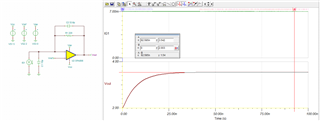
    Here is a design for the OPA856, that makes use of the 220 ohm feedback resistor as your transimpedance gain, 15pF photodiode capacitance, and the calculated feedback capacitance.

    OPA856_TIA_E2E.TSC

    Please let me know if you have any further questions about the design or if you need support on any changes to this design to meet the application requirements.

    Thanks,

    Nick

  • Hi Nick,

    Thanks for your quick answer. Is it possible to have the circuit design for the Spice software (to have the feedback capacitance value) or just a sreenshot of the design ?
    Is it a problem if the OPA856 spice model has only 5 pins ? (missing the NC, PD and FB).
    Is this OPA suitable for transimpedance configuration ? And if so, what are the minimum feedback resistance values in transimpedance configuration and in voltage voltage configuration in order to be in 1V/V minimum stable gain regime ?

    Thanks a lot,

    Adrien

  • Hi Adrien,

    The OPA856 is suitable for transimpedance configurations. I recommend checking out section 9.2 of the datasheet as there is some good information on using this device in a TIA configuration. As you have mentioned, the OPA856 has a minimum stable gain of 1V/V. In order to ensure you are operating above the minimum stable gain, you can check the noise gain of the amplifier. For TIA circuits, the noise gain will be NG=1+(Zf/Zg). At DC frequencies, the gain will be set by the feedback resistor. At high frequencies, the gain will be 1+(Cf/Cin), where Cin is the photodiode capacitance, op amp input capacitance, and stray PCB capacitance. Therefore, you should always be operating above the minimum stable gain for 1V/V using the values I provided in the simulation above.

    To address your questions about the model itself:

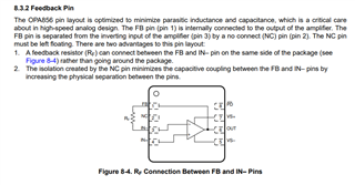
    • Any of our spice models will not include the No Connect (NC) pins or the Feedback (FB) pins. The FB pin is not included in our device models because it can easily be wired in simulation. Some devices have FB pins for real world layout purposes. The FB pin provides an internal connection from Vout to the FB pin and the FB pin is typically very close to Vin- so that the feedback network can be placed close to the device to reduce any stray capacitance by eliminating the need for large traces routing around the device. This snippet of the datasheet provides more information on this as well as the NC pin.

    • The model for the OPA856 also does not include any power down (PD) functionality. If you need to be able to turn on and off the device in simulation of a signal chain, you could use a switch connected to the Vs+ and Vs- pins to disconnect the power rails. Please note that since PD functionality is not modeled, any power down behavior in simulation can not be guaranteed.
    • In the simulation I have provided above, C1 represents the photodiode capacitance, C2 is the feedback capacitance, R1 is the feedback resistor, and the current source represents the output current waveform of the photodiode. If you prefer to use a SPICE simulator, the same configuration that I have shown in my previous post can be replicated.

    Please let me know if you have any questions.

    Thanks,

    Nick