This thread has been locked.

If you have a related question, please click the "Ask a related question" button in the top right corner. The newly created question will be automatically linked to this question.

OPA814: the edge-triggered ESD absorption devices across the supply pins

Part Number: OPA814

Hi team

Looking at the datasheet, there is a description as below. Could you tell what the edge-triggered ESD absorption devices mean? The edge-triggered ESD absorption devices are inside the device or outside of devices?

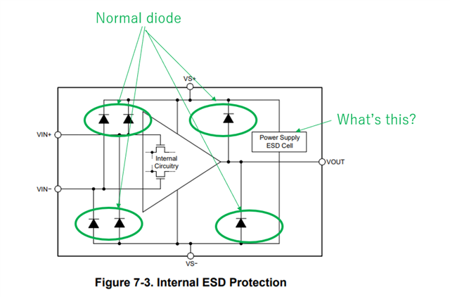
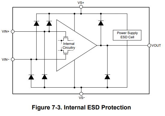
And what is the difference between the edge-triggered ESD absorption devices and normal ESD protection diodes inside the device as below?
Regards,

Noriyuki Takahashi

  • Hi team

    I am not sure that the diffrence the normal diode,  the edge-triggered ESD absorption devices and the power supply cell as below.

    Regards,

    Noriyuki Takahashi

  • The absorption device is the "ESD cell" box.

    The ESD cell is not triggered by a high voltage, but by very high edge rates (which are typically for ESD events), and when triggered, clamps the supply to ground. This would not be useful during power up.

    Please note that 1 V/µs is unlikely to happen during a normal power up because the decoupling capacitors need to be charged.

  • Hi Noriyuki,

    As Clemens said the ESD cell is inside the device.

    By "edge-triggered ESD absorption devices" we mean that if the supply ramp is more than that specified in the datasheet (1V/us max for this device), the ESD cell will get turned on.

    For other devices where this is not mentioned, the ESD may support Supply ramp much higher than this.

    Regards

    Anant

  • Anant,

    Thanks for clarification.

    So I am still not sure why the turing on the ESD cell can lead to the device destruction. Could you please explain this?

    Regards,

    Noriyuki Takahashi

  • Hi Noriyuki,

    If the ESD cell get turned on it may result is a very large current through it, which may damage it. Give me a couple of days, I will check what's the max limit of the current through this esd cell which will be not cause any damage to the device.

    Regards

    Anant

  • The ESD absorbtion device is intended to steer ESD events to it during handling and away from the active circuitry. However, it is still there when soldered into the board and if triggered by the supply dV/dT will act as an instanteous short across the supply pins, normally not a desireable thing to do. Now it may only fry the absorption cell, but collateral damage to the active circuitry cannot be ruled out. There are many different kind of absorption cells, including those that are not edge triggered.