This thread has been locked.

If you have a related question, please click the "Ask a related question" button in the top right corner. The newly created question will be automatically linked to this question.

OPA567: Damage issue

Part Number: OPA567

Hi,

There is damage issue with high temperature.

With start, it works well but output gradually get worse and there is no output finally.

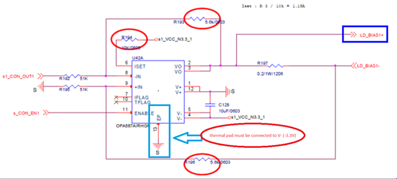
For LD operation, V+: GND, V-: -3.3V

The questions are:

1. if V- supply current rating is lower than requirement, it means V- supply voltage is not regulated. in this case, can OPA567 get damage?

2. if yes, could you explain why it get damage?

3. Now EP(pin13) is connected to GND. Is it ok that V+ also connected to GND?

Schematic is as below.
Thanks.

  • Hi David, 

    Is this inquiry related to the following thread that I replied last week?

    https://e2e.ti.com/support/amplifiers-group/amplifiers/f/amplifiers-forum/1324085/opa567-opa567/5043572#5043572

    It looks like that this is the same inquiry. Do you know if the OPA567's thermal lug or heat sink is connected or referenced to -3.3V?

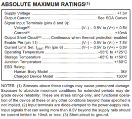
    Since this part is operating between -3.3V and GND, any of the input voltage exceeds the Absolute Max. Ratings could damage the part, even by a short duration. For instance, if someone is configured the input backwards, where non-inverting input exceeds (V+) +0.5V = 0.5V, then damage could occur. 

    I do not have these information with the customer from the inquiry. 

    Best,

    Raymond

  • The minimum supply voltage for OPA567 is 2.7V - powering the part from a lower supply voltage may result in a large shoot-thru current flowing in the output stage leading to damage. The thermal pad must be soldered to the PCB. The thermal pad should either be left floating or connected to V– and NOT to V+  as you show in your schematic.

  • Hi Marek,

    Resistance EP to V+ is 20MOhm and EP to V- is 1MOhm.

    There seems to be damage in EP to V-.

    You mentioned EP has to be connected V- or floating but it's connected to V+ in customer's schematic.

    Can it make this type of damage?

    Could you explain how EP, V+, V- is connected internally?

    Thanks.

  • Since p-substrate of the OPA567 die is internally biased at negative supply (-3.3V), external EP pad must also be connected to (V-) or left floating.  Any possible damage caused by wrong connection will depend on the type of die coat used to attached the die to the lead frame (conductive vs non-conductive).  But regardless, EP thermal pad of OPA567 may NEVER be connected to positive supply (V+) as this at best will result in long-term reliability of the product.