This thread has been locked.

If you have a related question, please click the "Ask a related question" button in the top right corner. The newly created question will be automatically linked to this question.

TLV9002:TLV9002simulation

Part Number: TLV9002
Other Parts Discussed in Thread: LMV358, TINA-TI

Hello, engineers!

I have a question regarding how to use the input/output rail-to-rail operational amplifier TLV9002IDR.  

I am simulating the circuit I want to design using TINA.

However, since there is no model for TLV9002, we are simulating it using LMV358.

This is what the TI homepage has recommended as an alternative.

I checked the specifications and it seems that everything except the input offset voltage is almost the same.

[Design overview]

Used in the analog circuit in front of the A/D converter.

Power supply voltage is 0V and 3.3V (3.3V is also the A/D reference) A voltage of 25mV, which is obtained by dividing 3.3V, is applied to the input voltage and used by the buffer amplifier.

Therefore, the output voltage will also be 25mV. (If there is no offset voltage etc.)

This results in a reference voltage of 25mV.

A bias voltage of 1.65V is often used when measuring AC voltage.

Think of this as 1.65V changed to 25mV.

The measurement target is a DC signal, a minute bias voltage used to compensate for near 0 in the A/D converter section.

The questions are below.

1) I am inputting a 25mV signal to the buffer amplifier, but the output is 31.09mV. What is this error?

I thought the error was about ±4mV.

2) Stable even when connected with a capacitive load of up to 10μF.

Can I trust this simulation result? (Since high frequency current flows through the operational amplifier output, a large capacity capacitor is connected.

Since it is stable with LMV358, I think it will be stable with TLV9002 as well.

Since the STEP signal is input, ringing occurs at the rise time, but this is of no concern. )

3) 1mADC flows into the output of this operational amplifier circuit. ⇒Sink operation with 1mA DC.

In addition to this direct current, an alternating current of about ±1mA/100kHz to 1MHz flows.

I am thinking of connecting a 5Ω dummy load to support sink operation of 25mV output voltage/1mADC.

I would like to use this method to ensure operation during low voltage/sink operation.

What do you think?

⇒Is it better to insert a diode to increase the operating point of the operational amplifier's output voltage?

In this case, of course, feedback is applied from the cathode.

"Yorosikuonegaisimasu"

BPZ_OPAMP.TSC

  • Hello Ishikawa-san,

    Great question.

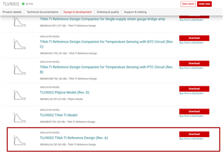
    The TLV9002 model is available under the TLV9002 product page in "Design & Development"

    I would recommend using TLV9002 as this device will be better suited for this application when compared to LMV358.

    2. Most devices will be unstable when operating with a 10uF capacitor. 

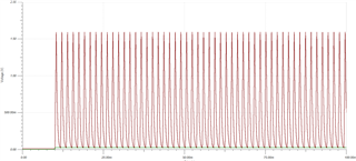
    I simulated your design and it looks to have sustained oscillations:


    If you are interested in learning more about op-amp stability, please consider looking over our stability series listed here: operational amplifier stability

    The best method to reduce these oscillations is to implement an RISO or RISO dual feedback design which will stabilize the heavy capacitive load.

    Does the ADC ref pin pull current constantly? This will help determine the best method for implementation.

    The voltage on the output looks higher than expected because the device is ruining into output swing limitations. The amplifier output can only swing so close to the supply rail, we call this "headroom" or output swing limitation. 

    Here are the output swing specifications for TLV9002: 

    As you can see, the amplifier will struggle to drive close to the supply rails of the device when driving higher current. 

    To confirm, you need 1mA continuous at 25mV above ground?

    This information will help we with revising the design to work well for your application.

    Thanks,

    Jacob

  • Jacob Nogaj san Hello! Unfortunately, I couldn't find the TLV9002 model.

    We are individually requesting support from Japan TI.

    From the contents of your contact, I understand that capacitive load (10μF) simulation with TLV9002 becomes unstable.

    It's just as I feared. I'm glad I listened.

    As you suggested, connect it to the capacitive load through the output resistor.

    I will apply negative feedback and local feedback (capacitor compensation) to ensure DC accuracy and stability.

    In addition, connect a dummy load to increase the output voltage level of TLV9002.

    (This will eliminate unnecessary worries such as swing restrictions)

    Design condition

    ・Input voltage 25mV @tlv9002 specs 0-0.1V=-0.1V ⇒OK

    ・TLV9002 operational amplifier output voltage > 1V

    @Determined by the amplifier's output series resistance and dummy load. ⇒OK

    ・Output voltage of the designed circuit =25mV=input voltage

    by the way,

    I am simulating with LMV358, but as shown in the attachment, even with a simple buffer, noise is superimposed on the output.

    It's synchronized with unrelated IG1.BPZ_OPAMP2.TSC

  • Hello Ishikawa-san,

    Here is the link to the TLV9002 TINA-TI model : sbomal3a (8).zip

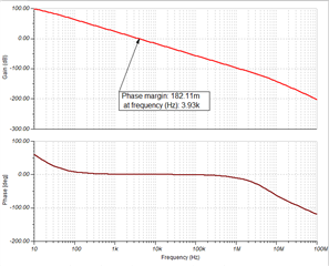
    Here is the phase margin without any compensation with RISO:

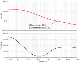
    After RISO dual feedback configurations:

    No need to use the pull down resistor to ground, this may cause more issues than it solves. 

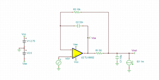
    Here is my circuit configuration:

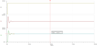
    This circuit works well for outputting 25mV in a stable manner even with 10uF on the output. 

    Here is the transient response:

    TLV9002_ADC_REF_Driver.TSC

    Please let me know if you have any questions.

    Best,

    Jacob

  • The circuit conditions are different.

    The direction of the current source used for the load is reversed. ⇒ Voa cannot be secured.

    Therefore, I think a load resistor is necessary.

  • Hello,

    Sorry for swapping the direction of current flow, I thought the amplifier was sourcing current into the ADC.

    Yes, in that case a load resistor will likely be the easiest way to sink this current and provide extra output swing to the amplifier. I would be cautious of putting low impedance loads on the output of the amplifier as this load can cause issues for the output stage of the amplifier if it ever had to buffer a voltage higher than 25mV. For this application, it should work.  

    Otherwise, you could use something like the LM7705 on the negative supply rail of the amplifier to help the device swing below ground (or sink current at low output voltages) on a single supply voltage rail. This would eliminate the low impedance load resistor, but would likely cost a bit more to implement. 

    Please let me know if you have any questions. 

    Best,

    Jacob