This thread has been locked.

If you have a related question, please click the "Ask a related question" button in the top right corner. The newly created question will be automatically linked to this question.

TLV9062: Drop in input signal when OP-Amp is powered on

Part Number: TLV9062
Other Parts Discussed in Thread: TINA-TI

Hi 

I am using TLV9056 as a differential amplifier to amplify the output from the current transformer (1:1000) the noninverting pin is biased with 3.3V and the Gain is ~50.

Refer to the schematic  below :
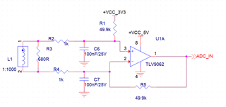
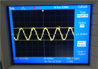
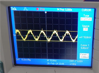
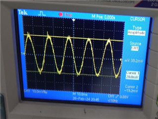
While testing, we observed that when OP-AMP is not powered ON there are no 3.3v and 5v on the circuit, the out of the CT measured across the R3 is as per design cals, but when the circuit is powered on the input differential voltage dips and with increasing in input voltage signal, the dip also increases.

Refer to the following waveforms : 

Test 1.

a. Waveform when the board is powered off. 
b.Waveform when the board is powered on. 
Test 2.

a. Waveform when the board is powered off. 
b.Waveform when the board is powered on. 
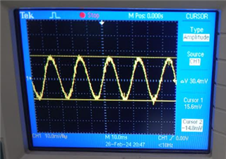
Test 3.

a. Waveform when the board is powered off. 
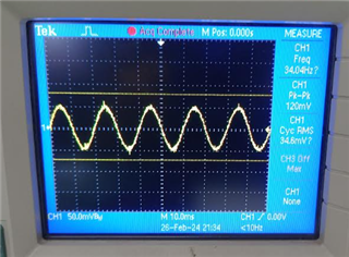
b.Waveform when the board is powered on. 
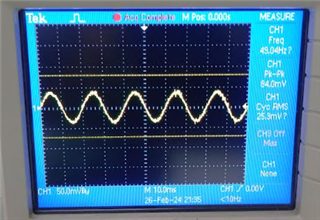
Please let me know the reason for this behavior and what is the workaround for the same. 

BR 

Chaitanya 

  • Hello Chaitanya,

    When disconnecting the supply rails, are you floating them or grounding them?

    If floating, the voltage will naturally be higher than non-floating as you are effectively turning a voltage divider into a high impedance terminal. 

    When you connect the op amp into the circuit with supply rails, the difference circuit acts as intended and creates the G=50V/V for the circuit. This closed loop gain equation requires R1 to terminate to a known voltage (3.3V) and R5 to go to the relatively low closed loop impedance of the op amp output terminal. In other words, this connection allows for current to pass, and consequently voltage to drop. 

    More importantly however, the .1uF capacitors will likely be causing issues in this circuit due to excessive capacitive loading at the inverting input to the device. This excessive capacitive loading will cause phase shift in our feedback signal, and can destabilize our amplifier. This will often look like oscillations on our amplifier output pin. 

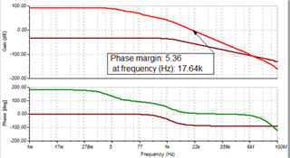
    I simulated the circuit in TINA-TI and I get a phase margin of just 5.3 degrees:

    We generally recommend greater than 45 degrees of phase margin to ensure stable operation over process variation and temperature. Our TIPL curriculum covers this idea in more detail, linked here: TIPL Stability

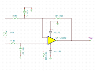
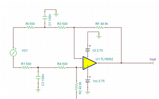
    I would recommend splitting the resistors into two separate sections with a capacitor in the middle: 

    See example below:

    Old:


    New:

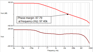
    After this change we go from 5.3 degrees of phase margin to 87.8 degrees of phase margin:

    This hardware change still allows for input filtering, and we maintain our closed loop DC gain of 50V/V.

    If this hardware change is not possible, I would recommend lowering the value of these capacitors to improve the stability of this circuit. 

    Please let me know if you have any questions.

    Best,

    Jacob