Because of the Thanksgiving holiday in the U.S., TI E2E™ design support forum responses may be delayed from November 25 through December 2. Thank you for your patience.

This thread has been locked.

If you have a related question, please click the "Ask a related question" button in the top right corner. The newly created question will be automatically linked to this question.

OPA2677: Bridge configuration for driving small peltier (tec)

Part Number: OPA2677
Other Parts Discussed in Thread: OPA567, OPA569, OPA2675

Hello,

I need to drive a small thermoelectric device (peltier) in order to control the temperature of a laser diode.  The peltier operating range is  +/- 100 mA with a compliance voltage of about +/- 400 mV.

The voltage for controlling the peltier current is provided by a DAC which has a max. output voltage of 5 V and a reset voltage of 2.5 V ("mid scale"). Further I'd like to use a single supply rail of 5 V.

I came up with a simple bridge setup consisting of two complementary inverting opamps. For the simulation, the peltier was represented by a 4 Ohm resistive load:
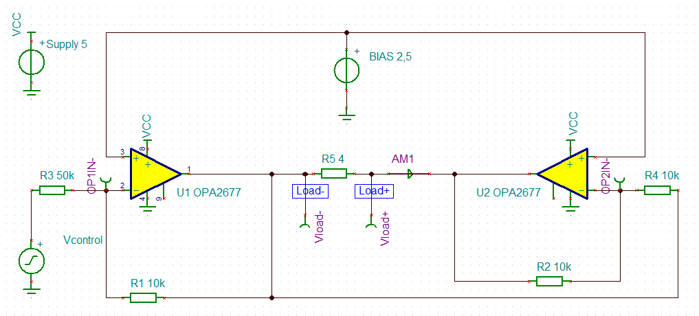
I calculated  Vload = Vload+ - Vload- = 2 * (Vcontrol - Vbias ) * G with Gain G = R1 / R2 and Vbias = 2,5 V.

To achieve a Vload = 0,5 V at a maximum DAC output of Vcontrol = 5 V, I calculated a gain of G = 0.1

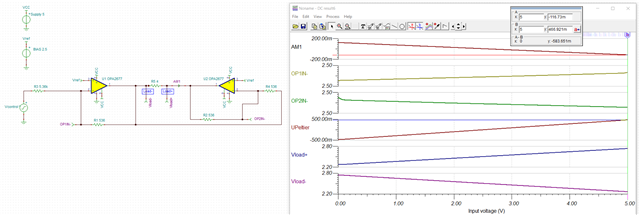
However, the simulation shows that a gain G = 0.2 is better in order to get the required output swing:

The graphs show that the negative inputs of both op amps  are close the the bias voltage at the positive inputs. This means the op amps are operating in their linear regime. The voltage at the peltier Vload ("UPeltier" in the graph) and the peltier current ("AM1" in the graph) cover the required range. It seems the design should meet the requirements described above.

Now my questions:

1. Why is my calculation off by about a factor of 2?

2. Could this work in reality (e.g., power dissipation, startup behavior) and have you comments regarding the design (e.g. op amp configuration, improvements to be made)?

3. I could only find three devices which would work in this design. I chose the OPA2677 as the other two (OPA567 and OPA569) are too "big" in my opinion. Can you suggest alternative devices for the OPA2677?

In case you want to run the simulation, this is the simulation file:


BridgeComplementaryInvertedOPA2677-G=0.2.TSC

Thanks a lot.

Dan

  • Hi Dan,

    Thank you for providing thorough information about your application as well as your simulation file.

    The formula that you are using for your calculations is correct, as shown in this application note (link). When replacing the OPA2677 models with an ideal op amp model in your simulation, the outputs show the expected results based on that formula.

    I am looking into if this is a model limitation or if there is some other cause for this behavior causing the output to be a factor of 2 of the expected results. I will work to get you an answer this week.

    Thanks,

    Nick

  • Hello ,

    Thanks for looking into my questions.

    I'd like to add that my knowledge regarding op amps is based on voltage feedback op amps.
    I noticed, though, that the OPA2677 is a current feedback op amp.
    I don't know if and what difference that makes for my application. The "Op amps for everyone" book states: "If you are trying to make a DC gain system, go back to voltage-feedback op amp. Current-feedback op amps have a lousy DC performance". Further it states "You have to use the value of RF recommended in the data sheet". As I take it, my application, i.e. temperature control, is to be located in the realm of DC performance. So I'm unsure whether the OPA2677 is the proper choice.

    Thanks.
    Dan

  • Hi Dan,

    Thanks for that catch. Yes, the OPA2677 is a current feedback op amp. In order to achieve the high output current drive that you are looking to achieve, you will need a current feedback amplifier as that architecture is able to achieve the larger output current levels. You can find more information about current feedback amplifiers in our TI Precision Labs videos.

    I adjusted the simulation to choose an Rf that approximately matches the noise gain of the system. In this case it is Rf = 536 ohms. With this change, the simulation matches the expected results.

    As you have mentioned, there are not a lot of options for amplifiers with that large of an output current drive. One other device you could look into is the OPA2675 which is also has a large output current drive. 

    Thanks,

    Nick

  • Hello ,

    Thanks for the suggestions. I changed the values of the feedback network resistors as you suggested and got the same results, results that match the calculation. Great! So I'll stick with this device.

    Regarding power dissipation, I calculated a maximum power of (5 V - 0.5 V) * 0.118 mA ≈ 0.5 Watt that has to be dissipated in the op amps. If I use the package with the ground pad ("DDA"), the thermal resistance is 55 °C/W. So I expect that the housing has a temperature of about 27°C above room temperature. That should be ok without an additional heat sink. Do you agree?

    Lastly, what about the startup behavior when the circuit is powered up? There are DACs that resets their output voltage to mid scale (= Vref). Using such a DAC to provide the control voltage Vcontrol means that there should be no current across the peltier when the circuit is powered on. Is that the way to go or  should the op amps be powered only after the DAC has a stable output voltage (which probably takes only some ms).

    Thanks!
    Best regards
    Dan

  • Hi Dan,

    In regards to the startup behavior of the circuit when it is powered up: There should be no issues with leaving the op amp powered up when the DAC is resetting the output voltage to mid scale, assuming that there is no large spikes in the output signal during that reset period while it is stabilizing. I also want to mention another key point. You should not power down an op amp if there is an input signal still present. Doing this could cause ESD diodes to turn on and source the current at the input of the device to the power supply rails in order to protect the internal circuitry. This could have potential catastrophic results for your signal chain. It is best practice to disconnect any input signal before powering down the op amp.

    In regards to the power dissipation: I recommend looking into the thermal analysis section on page 22 of the datasheet as it discusses how to compute the total internal power dissipation of the op amp. You are not considering the quiescent power and I am not sure that you are computing the maximum power dissipation in the op amp output stage to deliver power, though I would have to work through both calculations deeper to compare.

    Thanks,

    Nick

  • Dear ,

    Thank you for your response.

    You pointed to power down behavior. I understand that (also) during power up and down the abs. max. ratings need to be observed. You recommend "to disconnect any input signal before powering down the op amp." I am not sure how I should do this. Do you recommend to first power down the DAC and then the Op Amp?  Contrary to the power up event, the power down event is not really under my control. Currently there's no arrangement for a "power down procedure". Instead, the +5 V rail will "collapse" when the user removes power from the device. As the +5 V rail powers DAC, Vbias and the Op Amps, I hope that the input signal to the Op Amps will simply drop to GND with Vs.

    Regarding power dissipation, you pointed out that I need to take  "quiescent power" into account. That would be an additional PDQ = 5 V * 0.018 A ≈ 0.1 W. For calculating power dissipation in the output stage, PDL, I don't think that the assumptions in the datasheet ("grounded resistive load") apply to the bridged configuration here. Further, I have to admit that I don't understand the calculations in the datasheet, page 22. They seem contradictory to me: text states that output is fixed at  VS/2 (with VS = 6V) but at the same time text states output is at +2.5V; next, text emphasizes that "it is the power in the output stage and not into the load that determines internal power dissipation" but then calculates power dissipation in the load P = (VS/2)2/RL. Thus I tried to work it out myself, see above.

    I will check both issues with my first prototype.

    Best regards,
    Dan

  • Hi Dan,

    In order for the input signal to removed, you could put a relay between the DAC and the op amp that you can disconnect when you are ready to power down. Also, if you can not add a relay, then powering down the DAC first so that there is no output signal from the DAC when the op amp is the next reasonable solution. 

    I understand your point about calculating the power dissipated in the op amp because of the load. I believe that your previous calculation is correct and you should see about 0.5W of power dissipation. Then you would still need to add about 0.1W for quiescent power.

    Thanks,

    Nick

  • Hi Nick,

    Thanks for the prompt reply. I agree, I would not want to add a mechanical device like a relay to my design. Furthermore, as I mentioned, the power down event is not under my control. Thus I'd like to have a design that does not go all haywire or break when it is suddenly powered down.

    Thanks!
    Dan

  • Hi Dan,

    In the case of power down events not being in your control and the inability to place a relay or switch between the signal chain, it is recommended to limit the current being input into the op amp in order to limit the effects of any unexpected transient spikes caused from power down events by placing a current limiting resistor between the DAC and input of the op amp. There is a general baseline recommendation of limiting the input current to 1mA. However, in your prototype testing, you can do some power down event testing to determine what is best for your application.

    Thanks,

    Nick

  • Dear Nick,

    Thank you for your response. I think that R3 (5360 Ohm) in the circuit above can be considered the current limiting resistor which you recommended. Does that make sense to you?

    Best regards,
    Dan

  • Hi Dan,

    Apologies for the confusion, I did not catch that with my response. Yes, R3 would be the current limiting resistor in this case and it is large enough there is no major concern on the amount of current that would be input into the op amp.

    Thanks,

    Nick