This thread has been locked.

If you have a related question, please click the "Ask a related question" button in the top right corner. The newly created question will be automatically linked to this question.

THS4561: Differential amplifier output error

Part Number: THS4561
Other Parts Discussed in Thread: LMP2011, OPA2994, LM7332, TLV2333, OPA4354, INA826, OPA2810

Hi team,

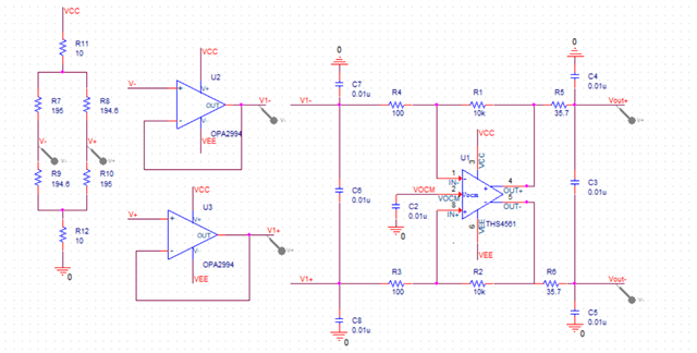
For our project we are using load cell. For amplifying the load cell output, the THS4561 amplifier circuit is used.

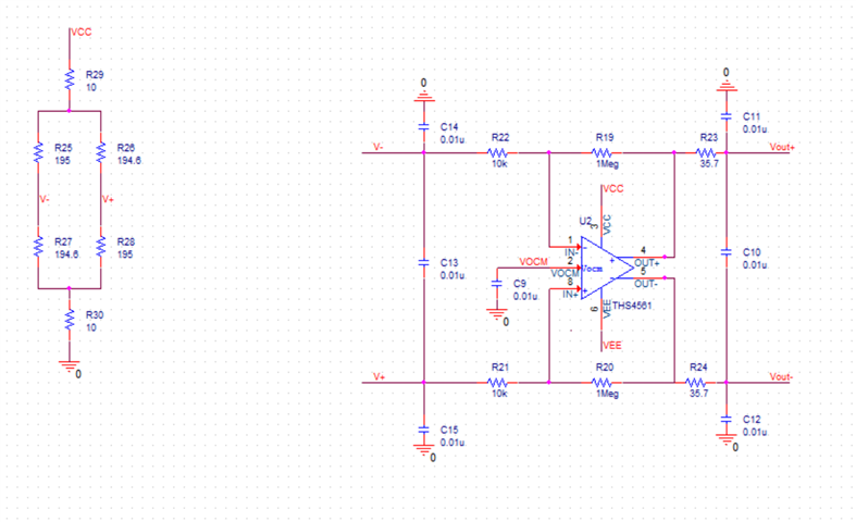
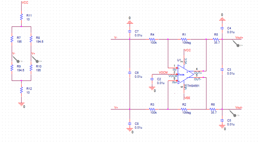
Refer the connection diagram given below, 

Ri=100k and Rf=10Meg
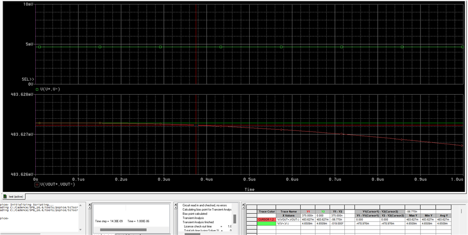
Output waveform
Theoretical:

Expected output = 4.65*100 = 465mV

Expected output = -4.65*100 = -465mV

Simulation outputs :

For positive input:

Diff Vi(V+ - V-) = 4.65mV
Diff Vout(Vout+ - Vout-) = 483mV

For negative input:

Diff Vi(V+ - V-) =  -4.65mV
Diff Vout(Vout+ - Vout-) =  -434mV

There is +18 mV and -31mV voltage difference between the expected output and simulation output.

Is this circuit correct or else what changes do I need to get the expected output?

Thanks.

  • Hi Sneha,

    I was looking over your circuit and I was wondering if you could confirm what the supplies of the amplifier are. One suggestion would be to reduce the feedback network resistor values. Offsets do occur due to bias current, which are amplified by large resistor values. Trying something like 10k and 100 should help with this offset.

    Best Regards,

    Ignacio

  • Hi Ignacio,

    Thanks for your response.

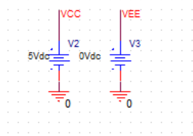
    Voltage source:

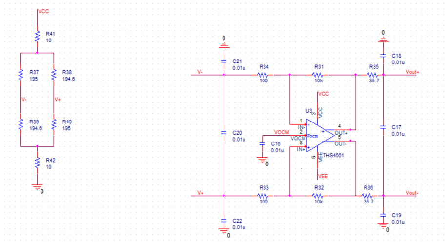
    We have tried the circuit for 100 ohms and 10k resistors.

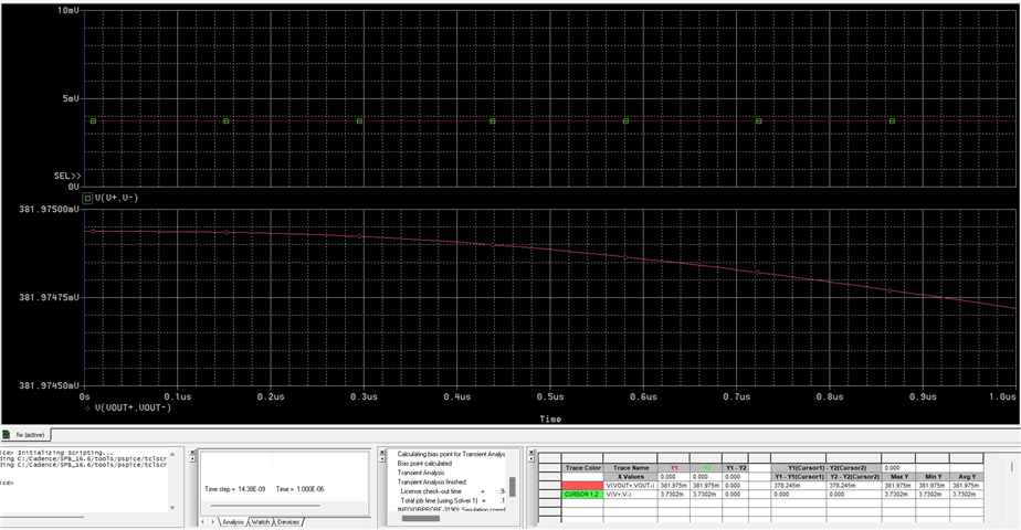
    Type 1: Ri=100 Rf=10k:

    Diff Vi(V+ - V-) = 3.73mV
    Diff Vout(Vout+ - Vout-) = 381.975mV

    Expected output = 3.73*100 = 373mV


    Type 2: Ri=10k Rf=1Meg:

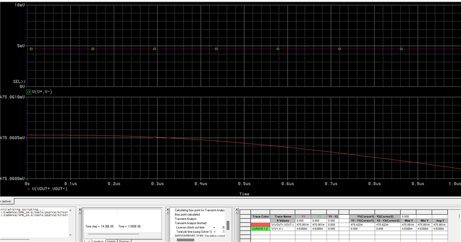
    Diff Vi(V+ - V-) = 4.63mV
    Diff Vout(Vout+ - Vout-) = 475.061mV

    Expected output = 3.73*100 = 373mV


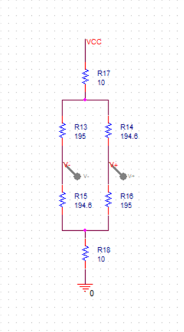
    Wheatstone bridge/Load cell alone :

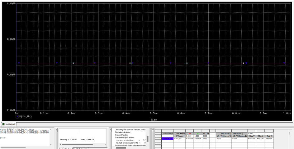
    The voltage of the bridge/Load cell whenever executed alone is 4.6532mV.

    In simulation, The load cell voltage drops whenever connected with the amplifier circuit(Type 1 and Type 2).

    Input side voltage(V+ - V-) drop of 0.923mV (3.73mV instead of 4.6532mV) and 0.023mV(4.63mV instead of 4.6532mV) respectively.

    Note: In previously shared circuit using Ri=100k and Rf=1Meg, we didn't face any input side voltage drop issues rather than output accuracy.

    Kindly suggest some ideas to meet the expected output without any voltage drop.

  • Hi Sneha,

    Thank you for the detailed description of the application, to limit any loading effects the best option is to implement an instrumentation amplifier. The very high input impedance will help limit this voltage drop and is ideal for a load cell application. I attached three articles below that highlight this type of amplifier and discuss options of building a discrete version or an integrated version which we also offer.

    Best Regards,

    Ignacio

  • Hi Ignacio,

    Thanks for your response.

    I need to read negative values as well.

    Below are the key parameters for our design,

    1. Load cell supply voltage = 5V, 

    2. Load cell output voltage = 1 mV/V; for 5 volts, max output is 5 mV and min output is -5 mV.

    3. The ADC's AVDD supply is 3V. Because the output of the amplifier is connected to the ADC.

    4. So the Gain is Output/Input = 3V/5mV = 600.

    As INAs are single ended, I need to detect negative values also.

    Kindly share your insights on this!

  • Hi Sneha,

    With an INA configuration in a single supply, you could still set a voltage to bias the output of the INA to mid-supply. This would allow differential measurements in both positive and negative directions. If you are looking for a solution with an FDA, you could consider buffering the inputs to remove the error from loading the signal source.

    Best Regards,

    Ignacio

  • Hi Ignacio,

    Thanks for your response.

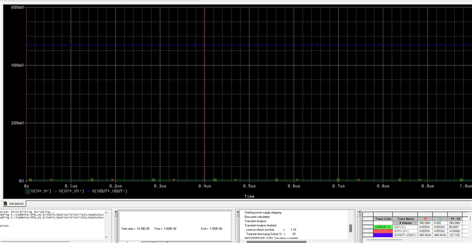
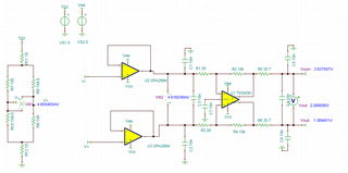
    1. For THS4561, I tried using LMP2011,OPA2994,TLV2333 and LM7332 as buffer for inputs. There was no voltage drop on the input side but I'm not getting the expected output.

    THS4561 with buffer OPA2994 Circuit with Gain 100 and VCC=5V:

    When VCC=5V VEE=0V:

    Differential Input (V+ - V-) = 4.6555mV

    Expected Differential Output (Vout - VRef) = 4.6555*100 = 465.55V

    Simulated Differential Output (Vout - VRef) = 469.45V

    Difference = 3.90V

    This difference changes for different Differential Input and ranges from 1V to 9 V.

    When I give VCC=3V or Gain = 500 ,the simulation result window does not pop out.

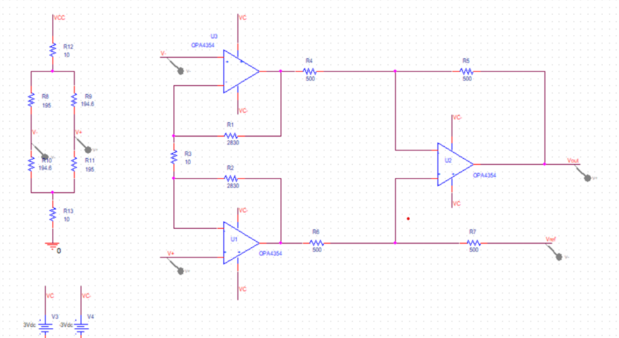
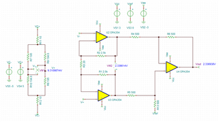
    2. For INA, I tried using INA826,OPA235,OPA4354,ADA4945 and AD620. There was no voltage drop on the input side and I'm getting expected output for Supply voltage 5V and Gain 100. I'm not getting expected output when Supply voltage is 3V and Gain is 500(which is my requirement).

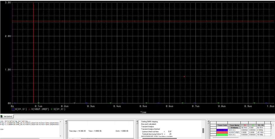
    OPA4354 Circuit with Gain 500 and VCC=5V:

    When VC=5V VC- = -5V VRef=2.5V:

    Differential Input (V+ - V-) = 4.6555mV

    Expected Differential Output (Vout - VRef) = 4.6555*500 = 2.3277V

    Simulated Differential Output (Vout - VRef) = 2.4508V

    Difference = 0.1231V


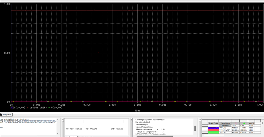
    When VC=3V VC-=-3V VRef=1.5V:

    Differential Input (V+ - V-) = 4.6555mV

    Expected Differential Output (Vout - VRef) = 4.6555*500 = 2.3277V

    Simulated Differential Output (Vout - VRef) = 939.961mV

    Difference = 1.3877V

    In the above circuit we can see that the output voltage error is higher when VC=3V.

    Kindly give your suggestions.

  • Hi Sneha,

    For the first circuit, there are two primary sources of error from the buffer stage and the FDA stage. To minimize the error from the buffer stage, I recommend implementing a FET input device that is more precise. One option would be something like the OPA2810. However, most of error will come from the FDA stage. The typical offset of the FDA is 50uV, however in a high gain configuration the offset at the output will be in the mV range which is what the simulation is showing. As for the setup you have, I did not have any issue setting the supplies to 3V, would you tell me what the VOCM pin is set to when you switch to VCC=3V? 

    For the second circuit, when you also change VC to 3V, are you adjusting VCC as well?

    Best Regards,

    Ignacio

  • Hi Ignacio,

    For the first circuit, we didn't set Vocm. Vocm (1.5V or 2.5V) was preset as the midpoint of the supply voltage (3V or 5V). For that configuration, we have connected the Vocm pin with a capacitor to ground.

    For the second circuit, VCC is 5V constant, we're varying VC as 3V and 5V.

    Kindly provide solution for this.

    Thanks!

  • Hello Sneha,

     Ignacio is out of office, but will return by tomorrow. In the meantime, I looked over your question and was wondering that for your INA, you have the supplies set to the same node, VC. Is this intentional? The negative supply should be at a lower potential compared to positive supply, and OPA4354 has a recommend max differential supply of 5.5V. Therefore VS+ and VS- is recommended not to be greater than 5.5 and has an absolute maximum of 7.5V.

     For the THS4561, Ignacio will be able to re-simulate with your Vocm setting, and get back to you shortly.

    Thank you,
    Sima

  • Hi Sneha,

    For the circuit with the FDA, I was able to get a result when changing the supplies and gain. 

    For your second circuit, the reason you are getting erroneous results is because the output range of the device is limited so this also limits the difference across the two outputs. If you probe the outputs of the INA you will see one output railing in the gain of 500V/V with 3V supplies. While the model does seem to work with the supplies being higher than the recommended value in the datasheet, the device does have a supply limit like Sima mentioned. Therefore, the real device would not work in its current configuration with the gain and supplies used. Would you be able to set the inputs to mid supply? Meaning the load cell is currently forcing V+ and V- to around 2.5V. If instead of ground, the load cell was set to -5V, the inputs would be set to mid-supply and will help the outputs not rail. This would change the 4.655mV value but that could be accounted for in the gain of the circuit. 

    Best regards,

    Ignacio

  • Hi sima & Ignacio, 

    Thanks for the reply!

    We need the FDA or INA or PGA for the gain of 550.

    The supply voltage of the amplifier must be 3.3V and load cell's supply voltage is 5V only.

    Kindly suggest some amplifiers having good accuracy on 550 gain.

    Thanks!

  • Hi Sneha,

    With the voltage requirements you have mentioned it will be difficult to use an INA configuration as your output range is fairly limited. The FDA configuration could work however in such a high gain the offset of the FDA will be a relatively large source of error. I will look into our portfolio and get back to you with potential options.

    Best Regards,

    Ignacio

  • Hi Sneha,

    I was able to look into our devices and simulated a few with the +/- 3.3V supplies and 500V/V requirement and the biggest problem is the lack of head room. As for a potential device, the THS4561 will be the best device in terms of voltage offset as this will likely be the largest source of error in your design. This source of error is still a few millivolts in such a high gain, which you have mentioned is a concern for your application, however this is the most precise FDA we currently have in our portfolio.

    Best Regards,

    Ignacio

  • Hi Ignacio,

    Thanks for the support. Will check this on our application.