This thread has been locked.

If you have a related question, please click the "Ask a related question" button in the top right corner. The newly created question will be automatically linked to this question.

LMV321: Basic design for the amplifier and calculation for resistor values

Part Number: LMV321
Other Parts Discussed in Thread: LM321,

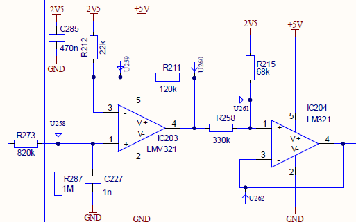
I have a basic op amp circuit diagram consisting of LMV321 and LM321 as shown below. The reference voltage for both OP Amp ICs are 2.5V. The input voltage is 5V. I want to re-design the circuit with 3.3V keeping same reference voltage of 2.5V. So, I basically want to know the design configuration and how the resistor values in the circuit are calculated. I have searched the datasheets of both op-amps, and I am left confused. Could you kindly provide a detailed calculation so that it will be helpful for the 3.3V design. The circuit diagram is shown below.

Regards,

Srinithi

  • Hi Srinithi, 

    Welcome to E2E! 

    Could you clarify a few items: 

    • What is the input stage before the LMV321 that is cut off in on the left side? 
    • What is directly connected to the output of the LM321? 
    • Which part of the circuit are you trying to re-design for 3.3V? The input into LMV321 (circled in green), the 2.5V reference (blue) or the supply voltage (yellow)? 

    Thank you!
    Best Regards,
    Ashley

  • Hi Ashley,

    Greetings.

    Many thanks for the response.

    Please find the responses for the following queries.

    • What is the input stage before the LMV321 that is cut off in on the left side? 

    The input stage before LMV321 is 1.2KHz/2.2KHz PWM signal from STM32G4 MCU.

    • What is directly connected to the output of the LM321? 

    The output of op-amp LM321 is directly connected to input of TI's analog switch 74HC4066

    • Which part of the circuit are you trying to re-design for 3.3V? The input into LMV321 (circled in green), the 2.5V reference (blue) or the supply voltage (yellow)? 

    I am trying to re-design for the supply voltage (highlighted in yellow)

    Regards,

    Srinithi

  • Hi Srinithi, 

    Thank you for the clarification on the schematic and re-design. 

    What are the desired input and output voltages that you are trying to achieve with the design? 

    Regards,
    Ashley

  • Hi Ashley,

    Many thanks once again for the response.

    The desired input is the HART signal of 4-20 mA having FSK signaling of 1.2KHz low frequency (for 4mA) and 2.2KHz high frequency (for 20mA) and voltage reference of 2.5V. The desired output voltage is 2.5V.

    Best Regards,
    Srinithi

  • Hi Srinithi, 

    One limitation to consider is the input and output limitations of the op amp when decreasing the supply voltage from 5V to 3.3V. 

    Please see the video here on Input/Output limitations for op amps: http://ti.com/video/6279999026001

    The LM321 has a limited upper headroom from the positive supply, so if you are using a lower supply voltage, the headroom for input and output on the upper end decreases. If you exceed this region, the op amp will behave non-linearly. If you need a wider range, then a rail-to-rail op amp is a better choice.

    Please let me know if you have further questions.
    Thank you!

    Best Regards,
    Ashley

  • Thank you Ashley for the valuable information.

    Regards,
    Srinithi