This thread has been locked.

If you have a related question, please click the "Ask a related question" button in the top right corner. The newly created question will be automatically linked to this question.

LM741QML: Inverting Amplifier Design

Part Number: LM741QML

Hi, I have been review the Texas Instrument's Application Report SLAA068B "Understanding Basic Analog – Ideal Op Amps". On page four (4) there is a drawing of a basic inverting amplifier. This drawing matches up with an inverting amplifier that I am working with with the exception of the R1 resistor (see drawing below) that attaches to the non-inverting input pin. I am think that R1 has been added to compensate for the Input Bias Current (IIB)  flowing into to or out of the non-inverting input pin. Is this correct?
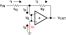
  • Hello Mike,

    Correct.  R1 is there to match the voltage change from IIB on the RF and RG resistors. R1 is also a additional noise source (like all resistors).

    R1 can also help protect the input if V- ever becomes positive or V+ becomes negative relative to ground (IN+ connection). 

    This could occur during power up, power down or during a supply or system fault.