Dear all,
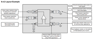
In the datasheet of the OPA838 there are the following recommendations for PCB layout:

1.Signal routing must be direct and as short as possible into and out of the op amp.
2. The feedback path must be short and direct avoiding vias if possible.
3. Ground or power planes must be removed from directly under the negative input and output pins of the amplifier.
But something is not clear for me, regarding the feedback trace:
It is mentioned that : Place feedback resistor on the bottom of PCB between pins 4 and 6:
Should I necessarily put the feedback resistor on the bottom layer? do I need to remove ground plane underneath the feedback trace as well?
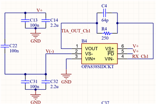
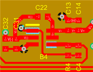
This is my current layout in a 8 layer PCB, so everything is on top layer, the feedback resistor and the capacitor in the feedback loop:
Schematic :

Layout:

Would you please share a reference PCB circuit deign file (Altium) or a general guide line for OPA layout that I can follow? The I can design a PCB with all the necessary considerations. Besides, I need some recommendation to improve my PCB layout.
Best regards,
Behnam,

