This thread has been locked.

If you have a related question, please click the "Ask a related question" button in the top right corner. The newly created question will be automatically linked to this question.

INA851: How to use noise figures for INA851

Part Number: INA851
Other Parts Discussed in Thread: PGA855

Hi,

The datasheet for the INA851 includes a 3.2nV/sqrt(Hz) figure and I am wondering how exactly to use that noise density with this device. I am wondering if I add feedback caps on using the FDA feedback pins to give the device a cutoff frequency, if that is the effective bandwidth for this calculation and multiplying 3.2nV by the square root of that frequency yields the noise. The datasheet includes some stuff that is confusing for me related to noise in the specifications section and footnote 7 says to consult the noise equivalent model section, but there is no noise equivalent model section?

Thanks,

ucy

  • Hello Lucy,

    Regarding the INA851 noise equivalent model:

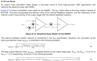
    Section 8.3.6 “Low Noise” on page 29 of the INA851 data sheet, provides a diagram and explanation of the simplified noise model for the INA851.

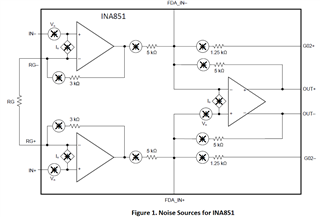
    The INA851 consists of a gain input stage followed by a Fully Differential Amplifier (FDA) output stage. Each amplifier in the circuit has a corresponding amplifier voltage noise and current noise contribution. In addition, the internal resistors have a thermal noise contribution. The Figure 1 shows the noise sources of the INA851.

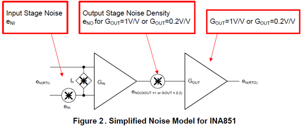
    The FDA output stage amplifier voltage noise source, current noise source and internal thermal resistor noise contributions are lumped into a single voltage noise source and represented as the eNO. The INA851 datasheet provides two specifications of eNO depending on the output stage gain, GOUT = 1 V/V or GOUT = 0.2 V/V. Similarly, the input stage resistor noise and voltage noise are lumped into a single voltage noise source at the input stage defined and represented as eNI. The current noise is kept separate at the input of the instrumentation amplifier. 

    Figure 2 shows the simplified noise model of the INA851:

    The simplified INA851 model uses a two-stage model; the designer needs to account for the gain at the input stage and gain at the output stage when calculating the total input referred noise and thee output referred noise.

    Equation 1 provides the calculation of the total input-referred noise density in nV/sqrt(Hz), eN(RTI).

    Equation 2 provided the total output-referred, noise density in nV/sqrt(Hz), eN(RTO). 

    INA851 intrinsic noise calculation example:

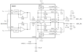
    Consider the circuit below, with GIN = 100V/V and GOUT = 1V/V, 1nF feedback capacitors, and a RC ADC low-pass charge kickback filter.

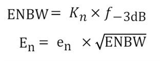
    Keep in mind, the noise bandwidth of the circuit is not the same as the signal bandwidth given by the filter corner, therefore the noise bandwidth must be corrected. Below is an approximation, which relates the Nth order low-pass filter response to the effective noise bandwidth (ENBW). The Kn constant is the brick-wall correction factor for a given Nth order low-pass filter. The Kn factor is 1.57 for a 1st order and 1.22 for a 2nd order low-pass filter respectively. The noise density is multiplied by the square root of the ENBW to calculate the noise in VRMS:

    In this circuit, the 1nF feedback capacitor with the 5kΩ internal feedback resistor forms a dominant pole at 31.8kHz, while the  pole of the ADC filter occurs at a much higher frequency.  Hence, the response can be roughly approximated to a 1st order filter with a Kn correction factor of 1.57. For more information about how this formula was derived, see the TI Precision Labs training series on operational amplifier noise (Op-Amp Noise: Calculating RMS Noise). 

    Using Excel, we can calculate the total intrinsic noise in µVRMS referred to the input or the output of the INA851:

    Below is an application note that discusses how to calculate the noise on the PGA855 programmable gain instrumentation amplifier.  Although the noise specs are different,  and the simplified noise model is simplified to a single stage amplifier, the application note provides much more detail in the noise calculations, and filter considerations.

    TECHNICAL DOCUMENT - APPLICATION NOTE

    Achieve High SNR with the PGA855, Fully Differential Programmable-Gain Amplifier

    Let me know if you have any questions.

    Thank you and Kind Regards,

    Luis Chioye