


Other Parts Discussed in Thread: OPA838,
Dear all,
I want to use a reference design form Texas instrument as a reference for my layout for OPA838, I noticed this reference design is a 4-layer board:
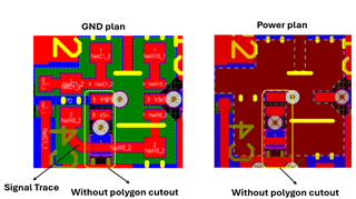
As we can see in the picture, there are polygon cutout both for GND and power plan, but I noticed, there is no polygon cutout for pin 5,6,2, which are positive and negative and enable pin, why we have kept GND and power plan underneath these pins?
My second questions is:
In this layout I can see under the signal trace (Signal Trace in the picture), we have discontinuously of the GND underneath the trace, can this cause any issue from layout standpoint? considering a s a genal rule for high speed routing we should provide a return path for signal trace, this return path is GND plan underneath the signal, but in this case we do not have it or we have it but in a discontinuous way. Please let me know if I'm right or not, if yes, how we can optimize the layout?
Regards,
