This thread has been locked.

If you have a related question, please click the "Ask a related question" button in the top right corner. The newly created question will be automatically linked to this question.

OPA2210: OPA2210

Part Number: OPA2210
Other Parts Discussed in Thread: OPA2328, OPA892, OPA992, OPA2992

Hi TI Design Support,

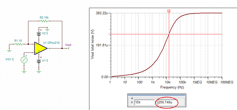
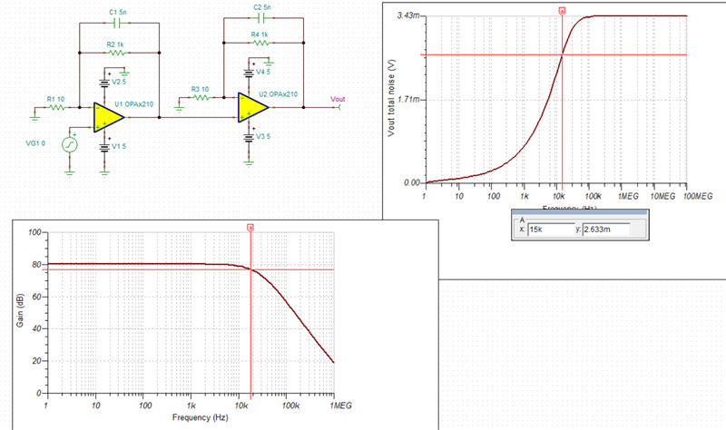
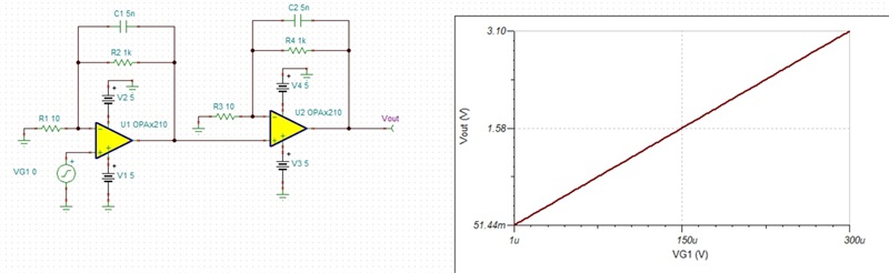
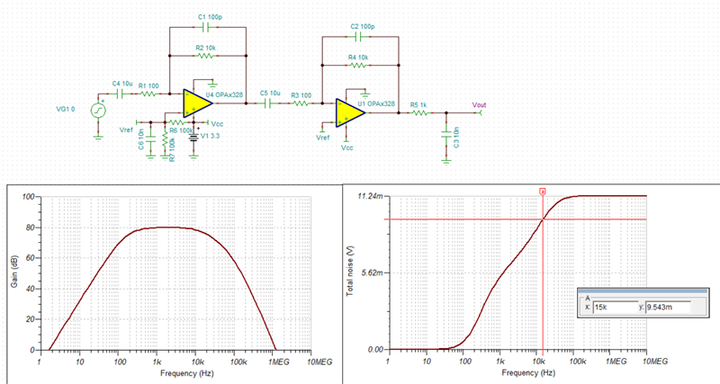
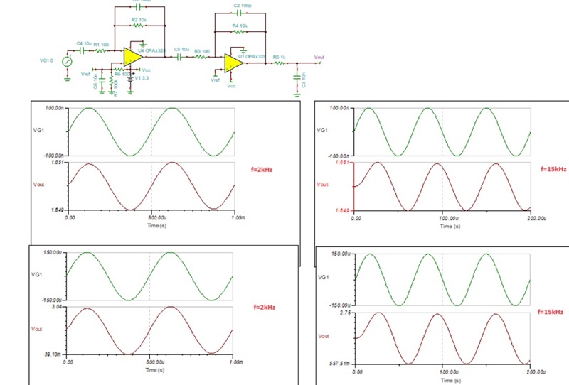
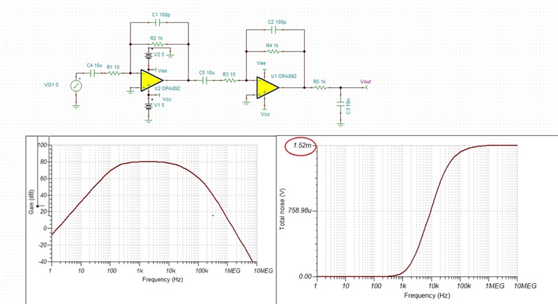
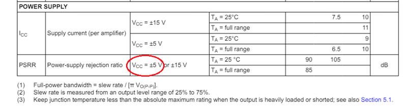
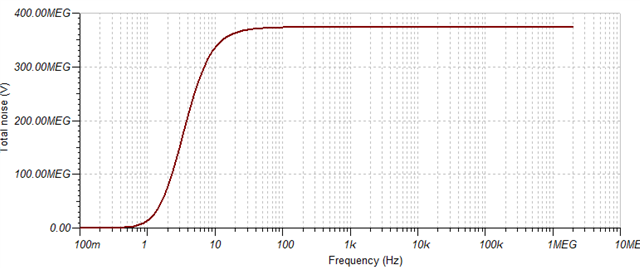
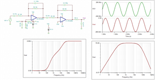
I have a sinusoidal and time varying signal which is in range of tens of nV to hundreds of microvolts, which I need to amplify to range of 0-3.3V, the environment is noisy, and the signal will be hidden in the noise. Can TI suggest me reference design or provide a design support for the same. My calculation says a gain of 100000 is needed, which may not be possible with single op-amp stage. The frequency of signal is 2KHz to 15 KHz. Please suggest and looking forward to discussion with TI.

  • Sumeet,

    There are several issues with what you try to do:

    1. If the signal is in hundreds of uV's, let's say 300uV, the highest gain you could use is 10,000 (not G=100,000)  resulting in the output of 3V .

    2. OPA2210 GBW is 18MHz resulting in the effective bandwidth of BW = GBW/Gain = 18MHz/100,000 = 180Hz for G=100,000 or BW=18MHz/10,000 = 1.8kHz for G=10,000.  Therefore, the circuit would be too slow for 15kHz input signal (thus, greatly attenuating Vout) unless you lower the gain down to G=1,000 resulting in BW=18kHz. 

    3. In the G=1,000, the output noise is 256uV (see below) - this means that the input refer noise would be 256nV.  Thus, the minimum input signal would need to be above 1uV to get decent signal-to-noise ratio. 

    Using two cascaded op amps in gain of 100 each, will result in the overall gain of 10,000 and bandwidth of 31.8kHz (fc=1/(2*Pi*RF*CF) - see below.  This results in the total output noise of 2.6mV that translates to 260nV input refer noise.

    The circuit would allow you to amplify 1uV to 300uV input signal as shown below.  Please make a note that the OPA2210 output linear range is 200mV above negative rail so if you plane to use a single supply this will further limit the minimum input voltage as you must also account for the max offset of +/-35uV.

    Last but not the least, OPA2210 minimum supply voltage is 4.5V (or +/-2.25V), thus you may NOT use 3.3V single supply - this will not work.  However, you may use +3.3V together with -1.2V - this will satisfy the minimum total supply of 4.5V and eliminate the concerns about violation of output linear range for low input signals.

    Sumeet OPA2210 application.TSC

  • Hello Marek,

    Thank you very much for your inputs, my requirement is that minimum signal that needs to be amplified is 100nV, please suggest me alternate part that would be more suitable for this application. My power supply constraints are 3.3V and I don't have a negative supply.

  • In order to work down to 3.3V single supply, you could use OPA2328 with output referenced at mid-supply (Vref=1.65V).  However, considering the total input referred noise is about 1uVrms (see below, Vin_noise=Vout_noise_total/Gain =~9.5mVrms/10,000 =~950nVrms), applying 100nv input signal will be swamped by the noise and there is not much you may do to fix this including using a different op amp - the input signal is just too low.

    AC coupling the signal as shown below results in following output waveforms for 2kHz and 15kHz sine input with 100nV and 150uV input signals. 

    This could be further optimized BUT detecting 100nV signal will be very difficult to obtain in roughly 10x higher noise floor environment.

    Sumeet OPA2328 application.TSC

  • Hi Marek,

    If I use OPA892, would I be able to get some hundreds of nanovolts amplified, I intend to use it in two stages, first one with gain of 1000 and cascade stage with gain of 100. Could you please let me know, if possible, a simulation file would be very helpful. My application requires very faint piezo signal to be amplified.

  • Sumeet,

    Assuming a bandpass filtering shown below, using OPA892 with its broadband noise below 1nV/rt-Hz would result is the input referred noise of around 152nVrms (1.52mV/10,000) and thus could be able to measure a piezo signal in hundreds of nV - see below.  BTW, as I mentioned before, a gain of 100,000 could NOT be used for upper range of the input signal in hundred of uV because it would require the output signal in tens of volts, which is not possible on 3.3V supply.

    However, OPA892 minimum supply voltage is specified as 10V (or +/-5V) and thus it would NOT work on 3.3V single supply - see below.

    Below I have attached OPA892 schematic for your customer's convenience.  Since OPA892 belongs to HSAMPS product line, please contact them for further assistance.

    Sumeet OPA928 application.TSC

  • Hello Marek,

    I created a charge amplifier using OPA992, I am attaching tina ti schematic, I am seeing very high noise levels, what is going wrong here?

    Please find attached schematic8507.RX_chargeAmp.TSC

  • Noise voltage is too high, can tell me what the problem is exactly, this doesn't seem to be plausible

    I am attaching the oscilloscope, it shows 0V output whereas It should show amplified sinewave?

  • Hi Sumeet,

    Marek is OOO. I can assist you. 

    If you changed the op amp from OPA2328 to OPA2992, here is the simulation, see the attached file. 

    Sumeet OPA992 application 06052024.TSC

    Please let me know if you have other questions. 

    Best,

    Raymond

  • Hello Raymond, I am using OPA 892 instead of 2992, Can you take a look at my file? I cannot use OPA 992, as noise profile of this opamp is not good. The tina spice file is attached to this message

    0636.RX_chargeAmp_OPA892.TSC

  • Hello Raymond, I am using OPA 892 instead of 2992, Can you take a look at my file? I cannot use OPA 992, as noise profile of this opamp is not good. The tina spice file is attached to this message

    8688.RX_chargeAmp_OPA892.TSC

    Please help me with this schematic, I am using OPA892 instead of 2992.

  • Hi Sumeet,

    I was able to look at the circuit you shared, and I am not sure how you are implementing the first stage. One concern as well is the very high Rf resistance. Due to bias currents, having such a high feedback resistance will cause an offset and will result in a saturated device. I would suggest starting out with the first stage as the addition of the remaining stages adds a higher level of complexity. I attached a reference for a charge amplifier circuit that shows how to design this type of circuit. The circuit highlighted will be a good starting point for your design.

    Best Regards,

    Ignacio

    Charge Amplifier Circuit (ti.com)

  • Thanks for your reply,

    The design you have given to me has receiver sensitivity parameter already set, however in my application piezo sensitivity is not known, I know it is hard to make guess, but that is also one of my reasons to get a charge amplifier instead of voltage mode.

    I get good output response till U2, as far as the circuit is considered it looks okay, It has something to do with ac analysis settings. Please have look at my design. Please let me know what is causing problems with AC analysis.

    6607.RX_chargeAmp_OPA892.TSC

  • Hi Sumeet,

    I was wondering if you could send the signal you are seeing at the output of the first stage? The device is not biased correctly as is resulting in erroneous results. On top of that, the minimum supplies required for this device is 9V, which will affect the devices performance.

    Best Regards,

    Ignacio