This thread has been locked.

If you have a related question, please click the "Ask a related question" button in the top right corner. The newly created question will be automatically linked to this question.

CIRCUIT060046: How to generate the AC analysis results as seen in SBOA325

Part Number: CIRCUIT060046
Other Parts Discussed in Thread: TINA-TI, TLV9102

Hello,

I just came across CIRCUIT060046: "High-side V-I with bipolar junction transistor (BJT) circuit"
I noticed that the description reads "This low-side voltage-to-current (V-I) converter delivers a well-regulated current to a load..."
I wonder what to call this circuit correctly: a high-side load or a low-side switch circuit?

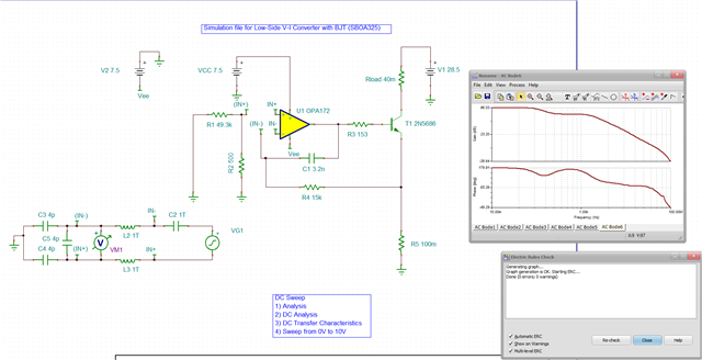
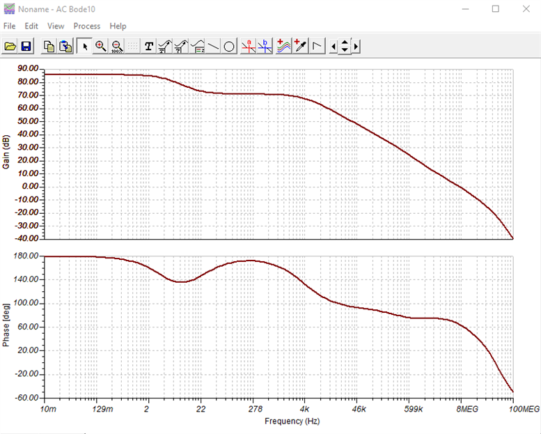
Anyhow, there's a design document available for this circuit, SBOA325Page 3 reproduces the results of an DC as well as an AC analysis run using Tina-TI.

I downloaded the model and could re-generate the "DC Simulation Results" as shown in SBOA325. 

However, I failed to re-generate the "AC Simulation Results". The AC analysis results look rather strange:

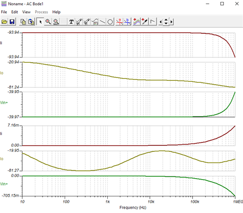
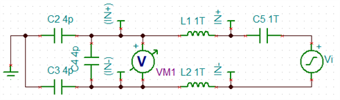
What am I doing wrong? I guess I have to manually add the proper curves using the post-processor feature.

Please advise.

Thanks.
Dan

  • Hey Daniel,

    To collect open loop data, you will need to open the feedback loop of the amplifier. However, where to break the loop can be tricky, but there is a method that works reliably.

    This output gives you the loaded Aol (aol-beta) from the AC simulation.

    Best,
    Jerry

  • Hi ,

    Thanks for your reply. I changed my circuit accordingly and now I get the same results as you do:

    I have some follow-up questions Slight smile

    Almost exactly the same curve. Although, I did not add the negative power supply Vee. How relevant is that?

    Further what exactly is this circuit below doing? I think I have seen it before but I don't really grasp all the details of it:

    This is my understanding of this circuit: The inputs to the op amp are split into "IN+" and "(IN+)"  (respectively for negative input) to break the feedback loop. Source Vi is AC coupled only (via C5) to the inputs of op amp "IN+" and "IN-". Feedback loop "(IN-)" and reference signal "(IN+)" are connected to the meter VM1.

    Why are L1 and L2  required? They seem to provide a DC only path between the inputs that have been split up. However, without L1 and L2 the AC analysis does not produce a result. 

    Why are C2, C3, C4 required? Without them I still see a result but it changes drastically.

    Further, our simulation results in a 0 db point at 8 MHz with a phase margin of +60°. The SBOA325 reports a phase margin of +78° at 237 kHz.  Why is this?

    Thanks a lot

    Best regards,
    Dan

    PS: Below is my Tina TI file attached.

    06 AC Simulation of 05.tsc

  • Hey Daniel,

    1. The negative supply is just something I do for a couple reasons. Generally our models converge better with a symmetrical supply, (this has no change on the output of the AC curve, it's just that the internal math is nicer/easier for the simulator to calculate when the supplies are symmetrical). The other reason is that it easily lets you set your op amp to a value inside the common-mode voltage range (CMVR). GND is almost always within the proper CMVR if your supplies are symmetrical, but this is not always the case for single supply. However, being outside your CMVR will yield a fairly obviously bad result (very large negative dB gain)

    2. L1 and L2 provide the DC bias path. If you simply opened up the loop, the output would slam to one of the rails and saturate, but if you let the op amp arrive at a DC bias point, but then open the loop for any practical frequency, you can get an open-loop measurement. This method also helps converge an integrator circuit. If you place only a capacitor in the feedback loop, a simulator will place an ideal capacitor, with no parasitic resistance. This will make the simulator see no DC feedback path on the amplifier, and it will rail the output. If you simulate down to a very low frequency value, lets say 1pHz, you will see where the open loop behavior of the inductor no longer holds true.

    3. C2, C3, and C4 give your input capacitance for the op amp. Without them you lose some of the behavior of a more realistic simulation. Since we are breaking the loop at the inputs, we need to re-introduce this capacitance to the feedback loop because it is now behind a 1TH inductor.
    4. There is a different op amp in the downloadable reference design compared to the PDF... Placing the TLV9102 (and it's appropriate input capacitance) will yield a similar bandwidth (247k). I'm not sure if they have used a different method to break the loop, you can get slightly different results based on how it was simulated.

    Best,
    Jerry

  • Hello ,

    Your thorough answer is very helpful. Thanks.

    I found your decoupling circuit also in other answers here in amplifier forum and Vi/VM1 are connected as you did.

    However, I just noticed that I "mounted" the voltage generator Vi and the voltage meter VM1 in reverse polarity compared to your decoupling circuit.Does that make any difference? I think it should not as I connected both the other way round.

    Thanks.
    Dan

  • Hey Daniel,

    I don't believe it would make a difference, as the large capacitor creates an AC short between the two inputs anyways, so the difference would just be the polarity of the input relative to the polarity of the voltage meter, as long as those are kept the same, it should be okay.

    Unsure if there are other repercussions but at first glance it seems ok.

    Best,
    Jerry