This thread has been locked.

If you have a related question, please click the "Ask a related question" button in the top right corner. The newly created question will be automatically linked to this question.

RCV420: Signal Conditioning for ADS131M08

Part Number: RCV420
Other Parts Discussed in Thread: ADS131M08, , TLV333, ADS1220, XTR111

Dear Team,

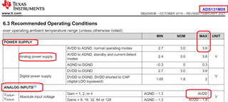
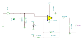
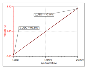
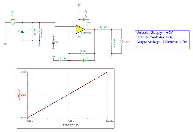
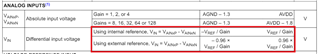
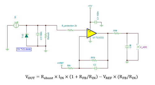
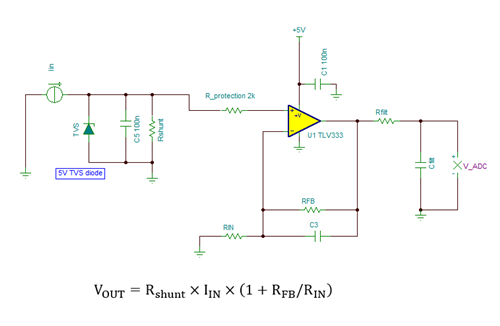
We have selected the ADC ADS131M08 but we have certain requirement of ADC for signal conditioning i.e I - V converter. could you suggest whether RCV420 is compatible for our requirement or some other part number which we can consider for signal conditioning for ADC with low cost ?

our voltage requirement is 0 - 5v.

Kindly check this and let me know.

Hoping to hear from you soon.

Thanks and Regards,

Prajwal Bhuse

design@avyannatech.com 

  • Hi Prajwal,

    The RCV420 is a legacy device.  If you want low cost, compact solution, you could easily use a discrete circuit with a precision amplifiers and resistors.

    Can you please clarify both the input current requirement and the output voltage requirement for the I-V converter?

    On your previous post, you have mention that you require an input current of 4-20mA.  Is this correct?

    On the post above, you mention that you require an output voltage requirement of 0V to 5V; however, the ADS131M08 only accepts an input voltage limited to the AVDD supply range, where the allowed range of the AVDD is from +2.7V to 3.6V maximum. Do you meant you need a voltage of 0V to 3.3V voltage instead?  See ADS121M08 spec below.

    For example, the I-V converter circuit below with the TLV333 precision op-amp is powered with a unipolar +3.3V supply.  The circuit accepts a 4mA-20mA input signal, and scales the output to ~100mV to +3.2V, allowing some headroom for op-amp output swing. This output voltage will be in the range of the ADS131M08 when the ADC is powered with a 3.3V supply. The circuit uses a shunt resistor of 160Ω and a TVS protection diode at the input of the op-amp. 

    TINA simulation file:

    forum_5-9-24b_tlv333.TSC

    Thank you and Regards,

    Luis 

  • Hi Luis,

    Thanks for your reply. could you suggest me alternative for RCV420 or share some document, design regarding the compact solution for discrete circuit ?

    our input current requirement is 4 - 20mA and output voltage requirement for I - V converter is 0 - 5v. as you mentioned above that  the ADS131M08 only accepts an input voltage limited to the AVDD supply range, where the allowed range of the AVDD is from +2.7V to 3.6V maximum. so, how can we achieve 0 - 5v  as our ADC'c VDD is upto 3.3v ? and if not, could you suggest some alternative I - V converter which will be fulfill our requirement ? 

    Kindly check this and let me know for any queries.

    Hoping to hear from you soon.

    Thanks for your support.

    Thanks and Regards,

    Prajwal Bhuse

    design@avyannatech.com

  • HI Prajhaw,

    As we have discussed, the ADS131M08 only supports an input voltage range of 3.6V maximum limited by a max 3.6V supply. Therefore, this ADC will not support a 5V input signal. If you need to support a 5V input signal into the ADC, you will need to replace the ADC device. On the previous post, I have provided an example of an I-V converter supporting +0.1V to +3.2V output voltage to properly interface with the ADS131M08, where the TLV333 is powered with the same 3.3V AVDD ADC supply.

    You can easily use the same TLV333 non-inverting amplifier circuit topology powered with 5V supply; and simply adjust the Rshunt resistor to 246Ω and R2 to 11.4kΩ resistor, to provide a max voltage of ~4.9V while powered with a +5V supply. However, you will need to replace the ADC for a device that supports a +5V supply.  See below I-V modified circuit powered with a +5V supply supporting 100mV to +4.9V output. 

    Thank you and Regards,

    Luis

  • Hi Luis,

    Thanks for your reply. 

    will it be okay if i use the same ADC i.e. ADS131M08 with above modified I - V circuit to achieve output voltage upto 4.9v ?

    Kindly check this and let me know.

    Thanks for your support,

    Thanks and Regards,

    Prajwal Bhuse

    design@avyannatech.com

  • Hi Prajwal,

    Luis is out today so I'll give some feedback here - if you use the ADS131M08, the max. input voltage is only 3.6 V.  You will not want to drive the ADS131M08 a voltage of 4.9 V.  But, Luis' circuit can be adjusted to either achieve 3.2 V out, or 4.9 V out.

    So, I would not recommend the above circuit, that outputs 4.9 V, to drive the ADS131M08.  I would use the modified circuit that outputs 3.2 V.

    Regards,
    Mike

  • HI Prajwal,

    The ADS131M08 ADC incorporates an internal voltage reference of 1.2V nominal.

    Hence, the full-scale range of the ADC is  ±VREF/Gain when using the internal reference. If using Gain=1, the full-scale range is  ±1.2V.

    If you wish to use the ADS131M08, since the ADC already incorporates a relatively high input impedance Programmable Gain Amplifier, (PGA) the most simple circuit will be to use a shunt resistor around ~60Ω that will scale the input voltage to +1.2V for 20mA, and +240mV for 4mA.  

    Hope this helps,

    Regards,

    Luis 

  • Hi Luis,

    Thanks for your reply. I've got the scenario of ADS131M08 with signal conditioning but my final concern is still pending. as per my requirement of voltage and current i.e 4 - 20mA and 0-5v, can i achieve this using the ADC ADS131M08 ? if not, do i need to change ADC or I - V for this requirement ?

    Kindly check this and let me know so i can proceed further.

    Awaiting for your reply.

    Thanks for your support.

    Thanks and Regards,

    Prajwal Bhuse

    design@avyannatech.com

  • HI Prajwal,

    I provided an I/V converter TLV333 circuit example that supports +5V output on the posts above; but as we discussed, it needs to be connected to an ADC that supports a full-scale range extending to +5V. The ADS131M08 full-scale voltage is limited to ±1.2V at G=1; and the ADC maximum supply is 3.6V; therefore, the ADS131M08 does not support a +5V input signal

    There are many ADCs that support full-scale range extending to +5V; one possible example could be the ADS1220; but there are many others. If you have questions about the ADCs, please submit a query on the Data Converters Forum, where the ADC applications team may have other suggestions.

    Thank you and Regards,  

    Luis


  • Hi Luis,

    Thanks for your reply. Still, I'm having questions regarding the same. the questions as follows:

    1. What will be the accuracy of conversion ?

    2. Can the circuit above of I - V conversion used for production? and this section will be used for industrial automation. So kindly suggest if any modification needs to be done?

    3. As mentioned in above schematic, a TVS diode is used for protection. Whether any isolation or protection circuitry required for the above I - V conversion circuit ?

    Kindly review this questions and let me know.

    Thanks for your support.

    Thanks and Regards,

    Prajwal Bhuse

    design@avyannatech.com

  • Hi Prajwal,

    1) The analog front-end consists of a shunt resistor followed by the TLV333 amplifier in the non-inverting configuration. The inverting path is referred to a reference voltage to shift the output to 0V when the input current is 4mA. The transfer function of the circuit can be written as below, where the resistors can be scaled for the required output voltage:

    The accuracy of the circuit above is a direct function of the % tolerance and drift specification of the shunt resistor and the RFB/RIN gain resistors, the accuracy of the reference voltage, and the offset and offset drift of the TLV333 op-amp.  Please note that the TLV333 has very low offset (2µV typical) and low offset drift 0.02 µV/C; hence the offset of the amplifier is not a dominant source of error. 

    If you don’t wish to use a reference voltage (VREF) to simplify the circuit, you could connect RIN to GND simplifying the circuit to the standard non-inverting configuration below.  In this case, the accuracy is a direct function of the  % tolerance and drift specification of the shunt resistor and the RFB/RIN gain resistors:

     If you would like to learn about error analysis. Please refer to the examples on the TI Precision Labs below.

    Statistics behind error analysis of ADC system

    2) You have requested a I-V receiver circuit similar the RCV420 when using the XTR111 3-wire current transmitter. On a standard 3-wire 4-20mA current transmitter-receiver configuration requires the transmitter and receiver to be connected to the same GND potential without isolation.

    If you need to learn about current transmitter types, please refer to the TI Precision Lab sections and resources below.

    Introduction to 4-20-mA current loop transmitters

    [FAQ] Designing with 4-20mA current loop transmitters (XTRs): FAQ links

     If your system requires isolation, the isolation is often done at the transmitter side, please review the XTR111 reference design using isolation below.

    XTR111: TIDA-01536,

    Single-Channel, Isolated, 3-Wire Current Loop Transmitter Reference Design Design Guide

    3) If the TLV333 op-amp circuit will be powered by a +5V supply, please use a TVS diode with a 5V reverse standoff voltage. The clamping voltage of the TVS diode will be at a voltage well above >5V, around ~10V or greater voltage depending on the TVS diode spec and current clamping condition.  Therefore, adding a series 2kΩ resistor at the non-inverting input will help limit the op-amp current to less than <10mA during a fault, at the TVS diode clamping voltage, protecting the op-amp during a fault.

    If you would like to learn about op-amp input protection, and TVS diode protection, please refer to the TI Precision Labs section tutorials below.

    Electrical overstress - Introduction

    Overstress protection

    Overstress: Selecting components

    Thank you and Regards,

    Luis

  • Hi Luis,

    Thanks for your reply. I'll check this and get back to you for any further queries.

    Thanks for your support.

    Thanks and Regards,

    Prajwal Bhuse

    design@avyannatech.com

  • HI Prajwal,

    Thank you,

    Kind Regards,

    Luis