This thread has been locked.

If you have a related question, please click the "Ask a related question" button in the top right corner. The newly created question will be automatically linked to this question.

OPA992: Op-amp as Non-inverting summing amplifier

Part Number: OPA992
Other Parts Discussed in Thread: ISO224

Hi,

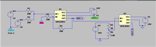
We are using OPA992 in our design as a summing amplifier.

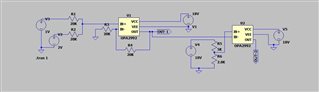
As per attached schematic we have done the design and PCB also fabricated.

During testing we are not getting the summing operation at 1st stage of Op-amp.

Please let us know is there any mistakes done in that circuitry.

  • What are the voltages at the input and output pins?

  • My input voltages are from 0.2V to 6V.

    Present I applied V1 = V2 = 0.6V.

    Output voltage is 18.2V same as VCC.

    For this input voltages, my expected output voltage is 1.2V.

    But it is not happening.

  • What are the voltages at the pins?

  • -IN pin voltages is 0.166V.

    +IN pin voltages is 0.535V.

    +VIN pin voltage is 18.68V.

    -VIN pin voltage is 0V.

    Out pin voltage is 18.68V.

    V1=0.602V, V2= 0.600V.

  • In theory, +IN should be the same 0.6 V.

    R4 and R3 form a voltage divider between the output and ground. In theory, the -IN voltage should be half the output voltage.

    It looks as if there are shorts on your board, or as if the OPA992 is damaged (try another chip).

  • We have done same implementation on one patch PCB.

    When we done common grounding for the V1, V2 and IC v+ the summing operation has done.

    But our measuring voltages are 5V gnd and our V+ is 18V gnd.

    If do the common ground it will effect some other IC's which are Isolated grounds.

    So, how can we solve this issue?

    Is there any requirement of Common grounding for input and Vcc Please confirm ?

    Please suggest any Isolation method to separate these two 18V gnd and 15V gnd if we do common both.

  • All voltages are measured relative to the OPA992's own ground (VEE/V−).

    If the two grounds have a fixed voltage difference, you might be able to use an amplifier with a wider common-mode range.
    Otherwise, you need an isolated amplifier like the ISO224.

  • Hello, 

    If do the common ground it will effect some other IC's which are Isolated grounds.

    So, how can we solve this issue?

    Please let me know if I am misinterpreting, is the blue, pink, and green grounds all different? 

    All the best,
    Carolina

  • Green and pink are same those are 18V ground.

    Blue is 5V ground.

    Iam using ISO224 for VDD1, 18V supply and ground.

    for VDD2 5V supply.

    If I connect common grounding it will affect this IC.

    Is there any method to isolate the common grounds ?

  • Hello,

    Understood on blue being a different ground than pink. 
    I think a solution can be reached by adjusting some of the passives. 

    Could you please specify the potential difference between pink ground and blue ground? Is it always the same? 

    All the best,
    Caro

  • Pink and Green Ground are same which are 18V Ground.

    Blue is 5V ground.

    Potential difference is 18 - 5 = 13V.

    Which passive components we need to use and what are its values please specify.

    Regards,

    Babu.M

  • Is there any method to separate the common ground signals.

    Our ground signals are 18V GND and 5V GND.

  • You have two different power supplies, but this does not imply anything about their grounds.

    How are these power supplies implemented? Do you actually know the offset between their grounds?

  • Hello Babu, 

    As Clemens has pointed out, I think there was a slight miscommunication. I understand the potential difference is 13V between the power supplies.

    What I would like to know is what is the potential difference between the two grounds. Is it a stable voltage value? Does it shift? Does it have a frequency?

    If my question is still not clear, please let me know and I will draw it. 

    All the best,
    Carolina

  • Hello Carolina,

    During schematic design Iam not grounded the Input side VDD1 ground and voltage divider low side ground.

    After common grounding of both voltage divider and VDD1 ground the IC is working

     .

    After common grounding of 300V input low and 18V ground the IC is working.