This thread has been locked.

If you have a related question, please click the "Ask a related question" button in the top right corner. The newly created question will be automatically linked to this question.

LOG200: Regarding the bandwidth of the logarithmic amplifier LOG200. replace AD8305

Part Number: LOG200
Other Parts Discussed in Thread: PSPICE-FOR-TI, LOG114, OPA335, OPA2335, OPA2197, OPA2191

Tool/software:

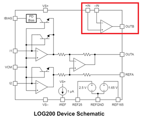
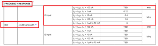
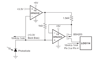
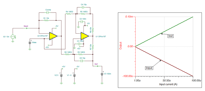
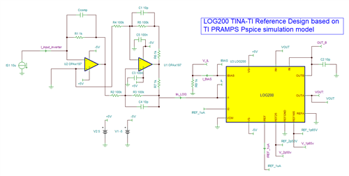
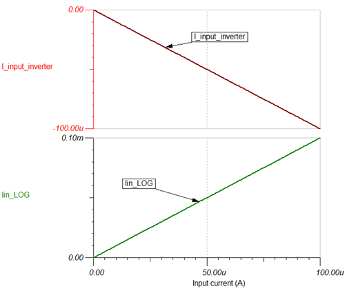
At present, our company is using AD8305 and looking for LOG200 to replace it. There is still little information about LOG200. I hope to get more information about it. The main point is about the bandwidth. The bandwidth of our optical system design is calculated to be up to 20MHz. In the logarithmic input part, I don’t know how to convert it. I know that the logarithmic amplifier will compress the bandwidth. The LOG_OUPUT_BANDWIDTH of LOG200 is 6MHz. How can I convert its maximum input bandwidth range? The same logarithmic amplifier AD8305 states that the maximum bandwidth is 15MHz. At present, the performance of our system is constantly improving, and we need to seek chips with better performance, so I need to get more information about LOG200 and logarithmic amplifiers.

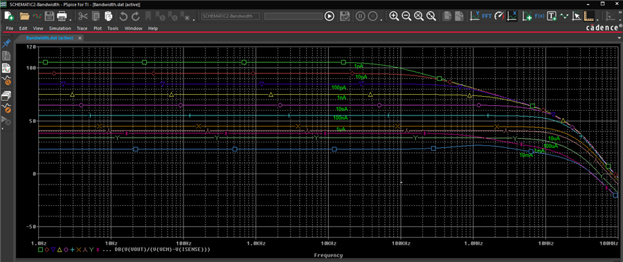
like this pic in AD8305's DataSheet.

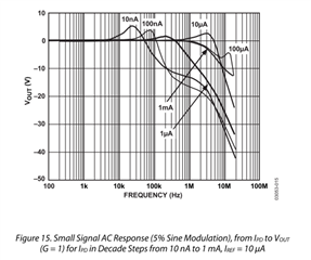
I am confused by its description in the datasheet. The GBW is shown as 42MHz, and the maximum bandwidth is written as 6MHz (-3db) elsewhere. This confuses me. Could u help me,plz

  • Hi Xander,

    As you have mentioned, the LOG200 is on Advance Information/Preview status; and the data sheet does not yet include all the final frequency specifications.

    I will need to discuss with the design team to provide you a preliminary or approximate plot of the AC frequency response of the device.  I will need to ask once available or approved by the team.

    What is the input range required in this application?

    What is the capacitance of your sensor or photodiode driving I1?

    I can provide support for the LOG200; but I can not comment on the AD8305, this device is from a different manufacturer.

    Regarding your last question, on the LOG200 data sheet, the Gain-Bandwidth Product (GBW) of 42-MHz is for the auxiliary operational amplifier OUTB, which is a separate op-amp with different frequency response than the logarithmic amplifier.  I will provide the feedback to the systems team to more clearly differentiate the specs; however the GBW spec is under the "Auxiliary Operational Amplifier" section.

    The datasheet does provide the typical -3dB BW for the logarithmic amplifier as a function of I1 current, while I2 is fixed to I2= IREF = 1uA.

    The datasheet does assume a parasitic CIN capacitance of 3pF or less (photosensor capacitance) on pin I1 for this specification.

    Thank you and Best Regards,

    Luis 

  • HI Xander,

    Using the preliminary LOG200 PSPICE-for-TI model, and performing the AC Bandwidth simulation, please find attached the AC frequency response of the LOG200 device. The I2 is fixed to IREF = 1uA.  I1 is set to to several decades in the pA  range to 10mA . 

    You can find the model for download on the link below.

    PSPICE-for-TI SIMULATION MODEL

    LOG200 PSpice Model

    Thank you and Kind Regards,

    Luis 

  • Thank u, Luis, I have another question. We use a photomultiplier tube to obtain the current signal, and its output is a negative current. Currently, we use the solution shown in the figure below to adjust the current direction. Do we also need to use this solution in LOG200?

    PMT: HAMAMATSU H10720 

    type: Current output

  • This solution is log114‘s DS Figure 9. Precision Current Inverter/Current Source.

  • HI Xander,

    Yes, the LOG200 can only accept currents flowing into the I1 pin in the range of 100pA to 10mA; hence since you require a logarithmic output as a function of a negative input current, you will  need to implement a current inverter.

    The current inverter circuit with the OPA335 and FET suggested on your post from the LOG114 data sheet can certainly work, we could consider replacing the OPA2335 with a more modern op-amp:

     Another current inverter I am familiar with, using a dual amplifier is below. The first stage is a transimpedance amplifier, followed by a Howland Current source stage. The transimpedance and Howland Current source gain will need to be adjusted to provide the proper gain or current output on your application.

    What is the expected current output range of the photomultiplier in your application?

    Are you using bipolar ±5V supplies or unipolar (0V and +5V) supply on your solution? What voltage is the VCM LOG200 biased to in the application?

    Thank you and Regards,

    Luis 

  • Hi, Louis,

    Our photomultiplier output range is 0-100uA and uses a bipolar ±5V supply. We will consider using the OPA2197 in our next design.

    Regarding VCM, we chose to connect it to GND and refer to Figure 8-5 for the design.

    Thank you,

    Xander

  • HI Xander, 

    I will take a look and provide you a quick circuit by tomorrow afternoon.

    Thank you and Regards,

    Luis

  • HI Xander,

    Attached is the TINA simulation for the OPA2197 circuit. It will easily handle the 0-100uA range on the application while powered with ±5V. You could also consider the OPA2191 that offers lower offset and offset drift; depending on the accuracy requirements in the same circuit.

    The Ccomp feedback capacitor of the transimpedance amplifier, (first OPAx19x stage), may need to be adjusted depending on the capacitance of the photomultiplier sensor.

    TINA Simulation:

    current_inverter_log200.TSC

    Thank you and Kind Regards,

    Luis