Part Number: OPA994
Tool/software:
Hello Tech Support,
I have two questions in regards to the OPAx994, being marketed as ", 24MHz, 125mA Output Current Op Amp With Unlimited Capacitive Load Drive", and specifically regarding its application of providing a split power rail from a single power rail, as per the article:
Title: "Split a voltage rail using an op amp to create a virtual ground"
Published 05-JUN- 2024
Authors: DAN TOOTH AND TYLER HOLMVIK
I am referring to Datasheet:
SBOSAF2B – JUNE 2023 – REVISED MARCH 2024
Question 1:
Section:
5.6 Electrical Characteristics
The test conditions for this section are stated as follows:
For VS = (V+) – (V–) = 2.7 V to 32 V (±1.35 V to ±16 V) at TA = 25°C,
RL = 10 kΩ connected to VS / 2, VCM = VS / 2, and
VOUT = VS / 2, unless otherwise noted.
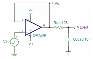
There are many entries there where the (a) load capacitance (Cload) and (b) Riso (the resistor interposed between op-amp output pin and load capacitor), are not specifically mentioned in the table.
For those entries, what are the applicable values for: (a) Cload, and (b) Riso?
Note: Cload and Riso are defined as per Datasheet fig 6.1, copied and pasted below for convenience:
Question 2:
Section:
5.7 Typical Characteristics (continued)
The test conditions for this section are stated as follows:
at TA = 25°C, VS = ±16V, VCM = VS / 2, RLOAD = 10 kΩ (unless otherwise noted)
These test conditions are mentioned at the start of the section, and repeated at the top of each page. Again, in several instances of the presented data, the values of (a) Cload, & (b) Riso are not explicitly mentioned.
What are the values for: (a) Cload, and (b) Riso?
Granted, many charts may not be affected by these two values, however, for the purpose of avoiding any doubt regarding test conditions, is it possible to disclose these values, given that that the product is being actively marketed as having "Unlimited Capacitive Load Drive".
If it is not possible to disclose this information in a general sense applicable to all charts in this section, then I would ask that this data is provided for the specific instances below:
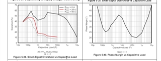
Referring to Fig 5-39.
Where was the overshoot measured from, was it (a) the output pin of the opamp, or (b) the other side of Riso ie: across Cload (ie: the node marked "Vout" in Fig 6.1)?
Referring to Fig 5-40 (Phase Margin vs Capacitive Load). This only has one trace, and the value of Riso is not explicitly provided.
Image below is from the datasheet, page 15.
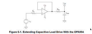
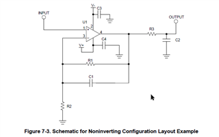
Further: in regards to Figs 5-39 & 5-40, what was the specific circuit used to test the device? I ask because datasheet Fig 7.3 shows the feedback network (R1, C1) is connected to the output pin of the op-amp, not the node marked as "output".
Thank you,