Because of the Thanksgiving holiday in the U.S., TI E2E™ design support forum responses may be delayed from November 25 through December 2. Thank you for your patience.

This thread has been locked.

If you have a related question, please click the "Ask a related question" button in the top right corner. The newly created question will be automatically linked to this question.

PGA855EVM: a technical defect

Part Number: PGA855EVM
Other Parts Discussed in Thread: PGA855,

Tool/software:

T05093738

Hi.

I recently received a defective part related to my purchase.

Description of the situation

1.
VS+ :+12V
Vs- : -5V

LVDD : + 5V

LVSS : -5V(VS랑 SMPS)

Gain : 1V/V

After Vin-, Vin+: Battery 1V connection, the input was measured as 0V,

Experiment with current limiting power (set of 1 volt, current 0.5A)

It has been determined to be an input current of 0.5 A CC.


2.
VS+ :+12V
Vs- : -12V (change -5V -> -12V)

LVDD : + 5V

LVSS : -5V(VS랑 SMPS)

Gain : 1V/V

Vin -, Vin + : Same as experiment 1


The conclusion is that the input terminal current is eating more than 0.5A.

Input Vin+, Vin- Not a short circuit when measuring resistance

It was not a short circuit when measuring Vin+ and Vin-resistance compared to GND.

In conclusion, it is judged that there is a problem on the PGA855 input terminal.

  • HI Dongsung,

    The PGA855EVM evaluation boards and PGA855 devices are tested during the manufacturing process, nevertheless, if you believe the evaluation board has a defect, and the device was purchased recently through www.ti.com or from an authorized TI distributor, please contact TI customer support.  

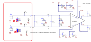
    Also, please verify that jumper J5 at the IN+ input, and J7 at the IN- inputs are placed in the correct position. These shunt jumpers need to be open and connected between pin 2-3 when applying an external input signal, and NOT shorted to GND on position pin 1-2.


    Thank you and Regards,

    Luis