A related question is a question created from another question. When the related question is created, it will be automatically linked to the original question.
If you have a related question, please click the "Ask a related question" button in the top right corner. The newly created question will be automatically linked to this question.
This is not something which is available in the datasheet, and should not significantly influence the op amp circuit design.
Slew rate will be determined by this capacitance, along with the current driver which charges the miller capacitor. I would recommend relying on the datasheet for slew rate values here.
Thank you for your reply. Does the LM358BA's internal capacitor have a significant impact on the circuit design of an op-amp, just like the LM358?
In a circuit configuration in which the output terminal of the LM358BA op-amp (+15V single power supply) is connected to the base terminal of a transistor, some op-amp output is unstable (called oscillation) and some is stable, even for LM358BAs from the same lot. Replacing the op-amp with an unstable output with another op-amp from the same lot stabilizes it.
As a countermeasure, we connected a capacitor between the negative input terminal and output terminal of the op-amp, which made it stable. Is the cause of this instability related to the op-amp's internal capacitor?
This internal capacitor indirectly influences stability.
Many internal op-amp parameters come together to determine the stability of the amplifier. External factors like circuit configuration can significantly influence the stability of your feedback system.
It is important to consider the phase margin of the amplifier in circuit design. It is possible that the circuit you are using has insufficient phase margin to reliably function in a stable manner. Phase margin is effectively the phase shift from 0 degrees relative from the output terminal to the inverting terminal. In a more intuitive way, this can be thought of as the margin in phase shift for how close a negative feedback system is from becoming a positive feedback system.
A 180 degree phase shift in a negative feedback system would be positive feedback, so 0 degrees of phase margin would be representative of a positive feedback system. Circuits with low phase margin exude behaviors which may include oscillations or ringing on the output.
Ideally, the circuit will have sufficient phase margin to operate over variations in process, and temperature. Generally speaking, 45 to 60 degrees of phase margin is recommended for most designs.
A feedback capacitor creates a second feedback path with low impedance for high frequency signals to pass through. This design method can be an effective strategy to help stabilize amplifiers, though it depends on amplifier configuration.
Can you please share your schematic? This can help me understand the configuration of the amplifier. With knowledge of your circuit design, we can simulate the phase margin for your circuit.
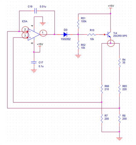
It looks like the NPN transistor forms a feedback path through the resistive load, and connects back to the inverting terminal. This would be your negative feedback path.
I am not able to runs any simulations as I require every component value to runs a stability analysis.
From a conceptual standpoint, this feedback capacitor can be thought of a parallel path which passes high frequency signals through C19 instead of passing through the transistor network.
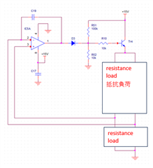
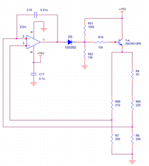
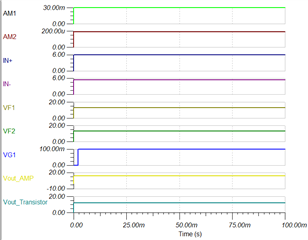
I have listed the respective constants in the circuit diagram. However, the resistance values of R65 and R66 are the resistance values before current is passed through them. The resistance value of these resistors changes when current is passed through them (the other resistors become normal resistors). When the circuit is stable, the resistance values of R65 and R66 are a few ohms higher than the listed values. Capacitor C19 (0.01μF) stabilizes the output of some op-amps, while it makes some op-amps unstable (known as oscillation).
I was able to run a simulation with a standard NPN transistor, but was not able to reproduce the oscillation. I did however see a large transient spike on IN+ upon startup.
C19 actually looks to make this transient worse. Can the customer change this to 100pF or less and test this change on their board?
Scope shots of the oscillation could be helpful to my testing.
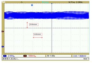
Regarding the capacitor, first there was oscillation when C19 was not connected. Next, I checked various capacitors below 100pF (for example 22pF, 100pF), but oscillation still occurred. The oscillation was improved by changing it to 0.01μF. However, there are still some oscillations even at 0.01μF.
I have attached the waveform of the oscillation state. Please check it.
I have imported the exact diode and NPN transistor the customer is using, but I am not able to reproduce any signs of instability:
It is likely that there is enough phase shift from the inverting input to the output of the transistor that the feedback signal is destabilizing the system.
Also, the feedback mechanism in this circuit is quite abnormal. In my simulations, the op-amp is operating more like a comparator, with output stuck at VOH with no change in output state.
Is the goal to create a current source through R65 and R66?
Knowing the goal and the load of the circuit can help me understand what I am capable of changing.
For fun, can the customer populate a 10uF capacitor for CF? I want to see if this further reduces oscillations.
As you pointed out, the op-amp behaves like a comparator. I confirmed that when the diode is not connected, the op-amp outputs a fixed amount at VOH. However, when the diode is connected, it oscillated.
The resistance of R65 and R66 changes when current is passed through them. The purpose is to stabilize the bridge circuit of R65, R66, R7, R8, and R4. In other words, R66 x R8 = R7 x (R4 + R65).
Thank you for the circuit description, this helps me.
Sorry for my designator switch. Yes, C19
Why does the circuit need this series diode?
I understand that this configuration effectively prevents current from back-feeding into the amplifier, but this circuit does not seem to have much risk of this condition.
Can the customer describe why D3 is included in the schematic?
I previously changed C19 to 0.1μF and 1μF, but the oscillation did not improve. Therefore, I have not tried 10μF, but it may not improve the oscillation.
As for the diode, as you pointed out, it is inserted to prevent current from flowing back into the amplifier. However, I previously shorted the diode, but the oscillation did not improve.
Thank you for the help here. I am sorry this debug is going so long, but I continue to struggle to recreate your issue in simulation.
Are you able to probe a few pins on the circuit? This will help me understand how the op amp is changing output states during the oscillation.
Here are the pins I am interested in analyzing:
I am now looking into the circuit in more details, and I am not certain the issue is the op amp destabilizing in the traditional sense. I suspect the amplifier is changing states very quickly and this causes a positive feedback to form and sustain the oscillations.
The capacitor in the feedback effectively creates an integrator circuit, this explains some of the results we see.
If this is the case, a LPF somewhere in the signal path may be beneficial. Otherwise, we may need to implement hysteresis to ensure the VOH-VOL transition has some guard banding to prevent rapid state changes.
However, the resistance values of R65 and R66 are the resistance values before current is passed through them.
Is the circuit's job to make R66 = R65 +30 ohms?
How can you be sure that feedback is negative when both "resistors" are variable with current? Can you elaborate why both need to be complex resistors?
Thank you for the simulation. I will check the pins you mentioned with an oscilloscope.
As you pointed out, there was a history of improving oscillation by inserting an LPF into the signal line. However, this method required changing the circuit, so it was not adopted. If the LPF is effective, does that mean that the phase compensation capacitor inside the op amp is also important?
How can you be sure that feedback is negative when both "resistors" are variable with current? Can you elaborate why both need to be complex resistors?
->I believe that positive feedback works properly, and negative feedback does not work properly. In other words, I believe that not working properly = negative feedback.
R65 and R66 are resistors that measure the ambient temperature and generate heat. It is a bridge circuit in which the amount of heat generated changes depending on the ambient temperature.
So as I understand, the circuit relies on using the resistors (R65 and R66) as heating elements, while also using the same components as components for controlling the feedback signal to the amplifier?
Yes, the LPF could help in realizing a more stable system. The phase compensation capacitor exists due to the inherent design of the amplifier. It is the configuration that the amplifier is being placed in which is causing the instability.
I am not able to simulate such a circuit as the feedback mechanism is controlled by eternal factors like temperature
Ron's point is that both resistors are capable of changing with respect to current. This circuit is not easy to stabilize without making changes to the op amp or the feedback loop.
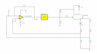
At closer examination, the circuit will force the bridge output to be zero (more accurately be Vos). This bridge canceling current flows through C19. In other words the amplifier doesn't simply read the bridge output voltage. It sets it, pin 2 is low impedance.
If you want to read the bridge output voltage and integrate out that error voltage, then add a new resistor from pin 2 to bridge. Its value should be at least 100X or more the impedance of the bridge output. At least 10k ohms. This will reduce C19 current, a good thing because LM358 can't change moderate current flow direction quickly. The new resistor will also slow the integration ramp, so you may need to reduce C19.