Other Parts Discussed in Thread: TL331, LM339, TL331LV,
Tool/software:
Hi team,
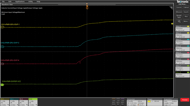
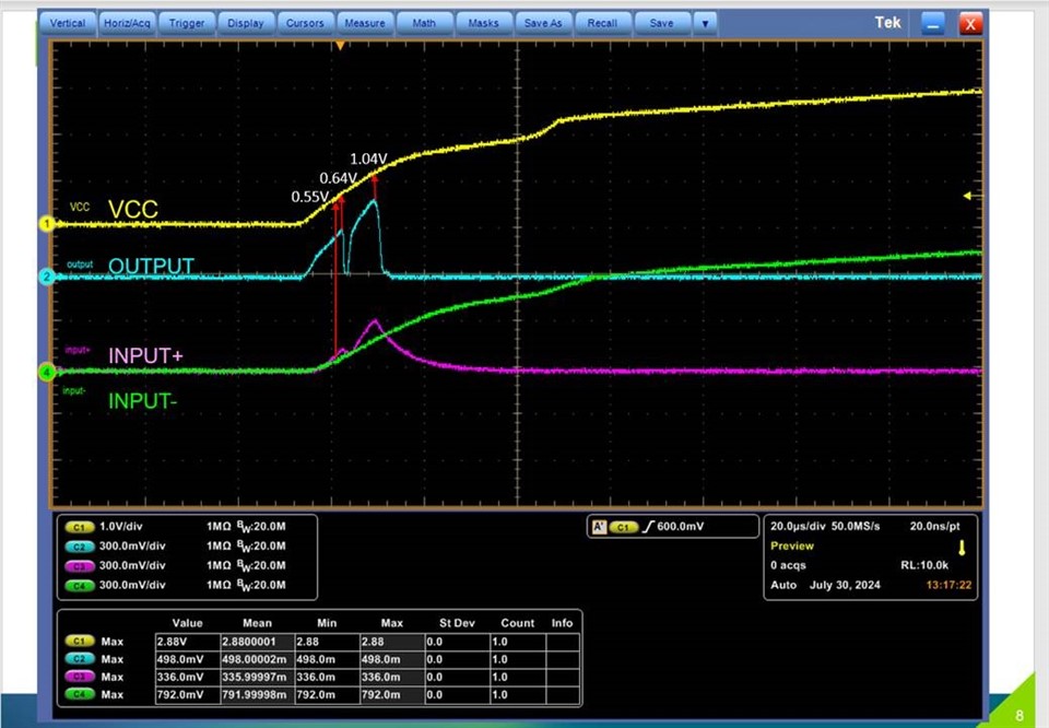
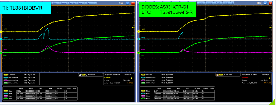
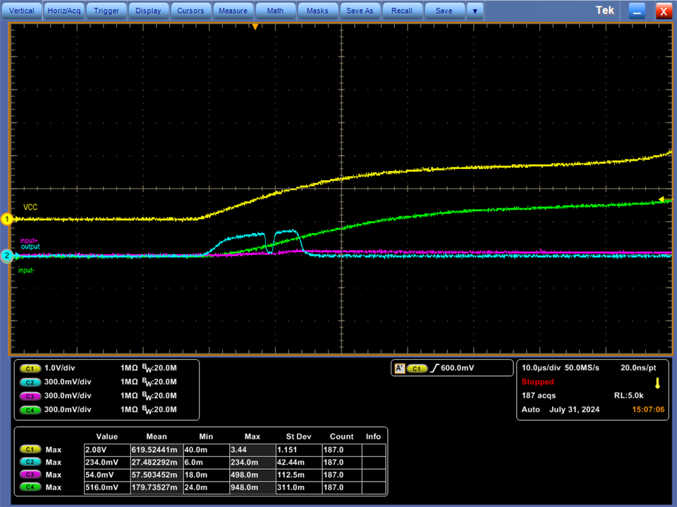
customer see in a fail rate around 7% that they saw all the input and output pins are pull high together with VCC, which is not the expected waveform .
is this because we don't have Power on reset or you think it's not cause?
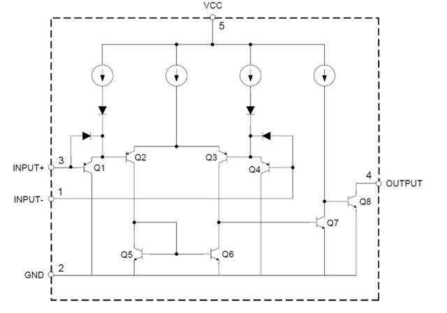
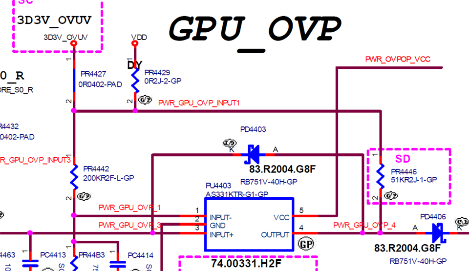
check PU4403 in below schematic