This thread has been locked.

If you have a related question, please click the "Ask a related question" button in the top right corner. The newly created question will be automatically linked to this question.

THS4551: Vocm pin connection capacitor?

Part Number: THS4551
Other Parts Discussed in Thread: TINA-TI

Tool/software:

Hello,

The THS2551 datasheet, p38 Section 9.4 recommends connecting a decoupling capacitor to the Vocm pin.

What would be a reasonable value for this?

My circuit uses 3.3V single rail supply and the Vocm is currently floating at ~1.6V.

The signals I am trying to amplify are low frequency (<20Hz).

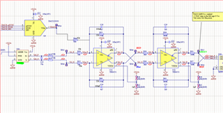
I currently have a 2 stage amplifier using this device where stage 1 has Rf = 470k, Ri = 100k Av = 4.7  and stage 2  has Rf = 680k, Ri = 1k0 Av= 680

The input signals are in the uV to nV range and I am currently trying to reduce noise on the amplifier output.
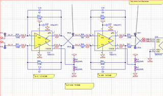
Thank you for any suggestions.

Best regards

B

  • Hi Bernt,

    The capacitor value we highlight in the datasheet is 1uF for the VOCM pin. For the actual circuit configuration, I was able to simulate the stages and it seems to show some stability problems due to the capacitors at the feedback. Is the noise you are capturing at the output random noise, or does it look like a sustained oscillation? If it is a sustained oscillation removing the capacitors at the feedback should stabilize the circuit. One suggestion would be to split the total gain evenly across the stages. This could help adjust the resistors easier as they are also too high and will result in other errors like offset due to bias current. I recommend sticking with the feedback resistor of 1kohms and adjust the gain resistors appropriately. This will also help reduce noise. Capturing a signal in the nV range will still be very difficult but reducing the resistors is one adjustment work considering. 

    Best Regards,

    Ignacio

  • Hello Ignacia,

    Thank you very much for the help and reply.

    I did add 1uF to the Vocm pin but it made no measurable difference.

    While waiting for your reply, I did more testing and shorted the inputs of stage1 together to see what happens to the noise.

    The noise stayed the same and after some more verification of power supply etc, I concluded that the circuit may be suffering from Johnson resistor noise. I thus replaced all stage 1 resistors fo become 1/10th of the original value. Rf= 22k and Ri =1k. I left the capacitors art.

    This seems to have resolved the noise problem.

    I then received your reply and I am now not sure if the noise was caused by Johnson noise or because of the simulated instability you mentioned. Either way, I have made progress.

    May I know how you simulated this? I tried before but the LTSpice will mostly not converge on the model for this chip and I could not get any usable results from that.

    The next p[roblem I observed is a very slow drift in offset. I observe this on the output of stage2 and calculating it back to input, it seems to be drifting ~400uV/minute. And always in one direction. I have not observed it long enough (tested for 1h) to see it if eventually stabilises.

    Again, when shorting the inputs of stage1, the slow drifting stops. I suspected the actual sensor causing this but measuring across the (un-shorted) inputs a uV capable meter, I do not see this kind of drift from the sensor.

    Could this be another instability?

    As you suggested, I will also change the gains of both stages to become more equal but have not yet done so yet.

    Best regards

    Bernt

  • Hi Bernt,

    The higher the Rf resistors in the feedback the more offset we can expect at the output. Reducing this will help with the absolute value but the drift is very interesting. We do expect offset drift as the temperature increases, does the device heat up during this test or is it at room temperature? It could be a stability problem but in the gain setting you described it is not showing any stability concerns. Just to confirm you removed the feedback capacitors from the FDA stages correct? I was getting low phase margin results when including these capacitors. One suggestion to help debug this circuit is that I would zero in on the first stage only, meaning remove the R30 and R36 resistors and leave off the next stages. When probing at the output of the first stage do you still see this offset drift? As for the simulation, I am using TINA-TI. You can download the simulation software for free off our website. I will attach the simulation file I am using for the stability simulation. 

    Best Regards,

    Ignacio

    THS4551_StabilitySim.TSC

  • Hi Ignacio,

    Thank again for the help.

    No, capacitors are not yet removed. I will do this today. They were intended to lower the bandwidth of the amplifier by fo < 10Hz.

    I tried to use the Tina application with your .TSC file but unfortunately I do not know how to use that program and it is much different to anything I have used before.  I have not made any useful observations or progress yet except that the amplifier does not like being in a offset compensated state i.e. Vdiff = 0.

    I have an offset compensation circuit with a DAC which appears to work but as soon as I get the output to be close to zero, it jumps past zero and into saturation on the opposite polarity.  It then takes several steps on the DAC to come out of saturation and start approaching zero again, only to repeat the problem but the other way. For whatever reason, there seems to be some sort of instability near zero or a sudden positive unwanted feedback.

    I am now wondering if injecting the single ended offset compensation only into 1 leg of the amplifier is causing something unforseen to happen.

    I did test by changing temperature with a small heat gun and that has a huge effect on the offset. It could be a or in fact  'the' reason for the drifting.

    BTW: I originally had the Ri input resistors 100k on stage 1 to keep the input impedance of the amplifier high.

    Since changing this to 10k, it is loading the sensor.

    This is a non ideal situation but I need to keep the component count down as this is a tiny end product where there is literally no space for much, even using 0402 parts.

    Here you can see the current arrangement for the offset adjustment.

    I will keep investigating and experimenting. I hope I can get this design to work in the end since I need it for a new product I am developing.

    Best regards

    Bernt

  • Hi Bernt,

    I would definitely start by removing these feedback capacitors as this is what is causing the phase margin to decrease. Would potentially filtering at the output of the stage be possible? As far as the compensation circuit, there is a chance the imbalance among the FDA branches could be causing the error you are seeing. We always recommend having balanced branches as any imbalance could result in things like distortion in a signal. The way we often adjust a circuit to have a high input impedance to an FDA is with buffer stage driving the inputs, but I fully understand the reason why that is not feasible. I was getting good phase margin results in the high gain using large Rg resistors, however noise is the concern with this configuration as well as offset due to the large Rf resistors.

    Best Regards,

    Ignacio