Because of the holidays, TI E2E™ design support forum responses will be delayed from Dec. 25 through Jan. 2. Thank you for your patience.

This thread has been locked.

If you have a related question, please click the "Ask a related question" button in the top right corner. The newly created question will be automatically linked to this question.

INA241A-Q1: INA241A-Q1

Part Number: INA241A-Q1

Tool/software:

Hi all.

I'm using INA241A3-Q1 shunt amplifier. I have some problem. We got boards from assembly. During testing one of INA241A3-Q1 has burnt:
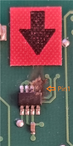
I'm trying to understand what could be a cause of it.

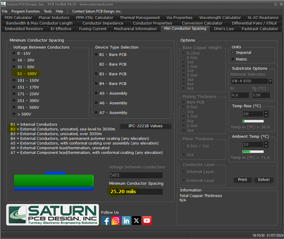
I've checked that there should be a minimum gap of about 25mils at an external layer (I'be used Saturn PCB):
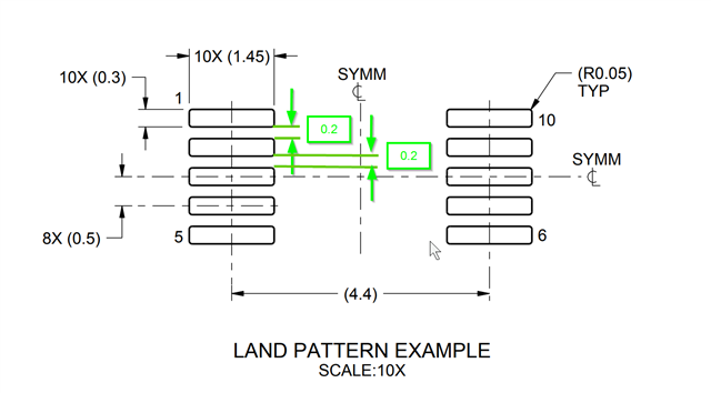
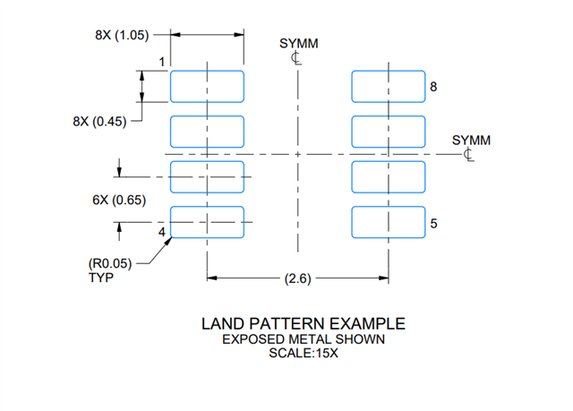
However, the recommended gap between adjacent pins according to datasheet is 0.2mm (8 mils):
This component is capable to withstand common mode voltages of up to 120V!

Since pin 1 is a "+" terminal, and pin 2 is GND, and according to clearance/creepage calculation it seems to be a problem.

I'm trying to investigate this problem, and woild like if someone has an idea.

Sincerely,

Alex

  • Alex,

    Yes per the IPC standards that is the case and this package does not meet it.   We are developing an alternative package for cases where the isolation standard is key in the application.  It is a larger package with a no connect pin between the Input pins and GND and Reference pin.  You can see this in the datasheet.  You can also use on of the other packages with larger spacing.

    Regards,

    Javier

  • Hello Javier,

    Thanks for a fast response.

    It looks like my fear regarding this fault was not unfounded.

    As I understand, only SOIC package can meet the clearance requirement for voltages 51V-100V.

    Do you have an idea for fixing an existing design? May be some coating?

    Alex.

  • Alex,

    I do not know of anything for this.  I think coating is one option but I am not sure what the limitations on that are as I have not done it.

    Regards,

    Javier

  • OK

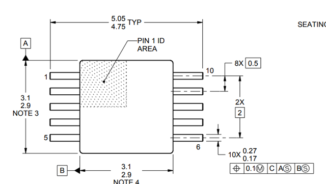
    By the way, I looked at an upcoming VSSOP-10 package. A gap between adjacent pads for this package is 8mil. Since there will be NC pin at the middle an aggregate gap will be 16mils, which is still less than standard requires (25mils). Am I missing something?

    Thanks,

    Alex.

  • Hello Alex,

    I calculated 0.2mm+0.3mm+0.2mm = 0.7mm = 27.5 mil.  If this is not enough you could also add a slot in the PCB, but the pin to pin with the variation in the package could be very close to these numbers as well.

  • Hello Javier,

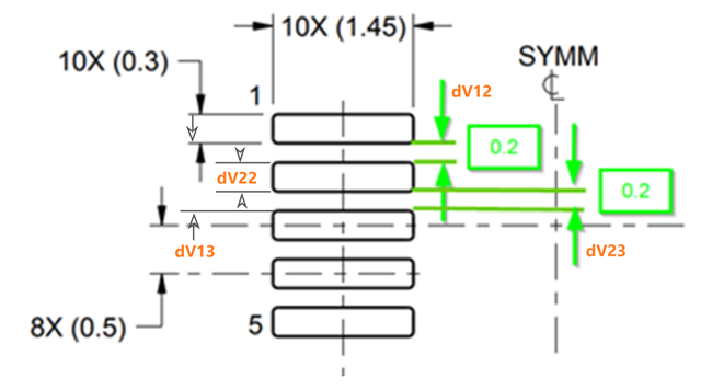
    I'll try to explain myself ... a voltage difference between pin 1 and pin 3 will be a sum of voltage differences, i.e.:

    dV13 = dV12 + dV22 + dV23

    Where:

    dV13 - Voltage difference between edge of pad 1 to edge of pad 3 (i.e. voltage of IN- to GND).

    dV12 - Voltage difference between edge of pad 1 to edge of pad 2 (i.e. voltage of IN- to NC).

    dV23 - Voltage difference between edge of pad 2 to edge of pad 3 (i.e. voltage of NC to GND).

    dV22 - Voltage difference between opposite edges of pad 2 (voltage across NC pad).

    Since pad / component's pin are made of conducting material dV22 can be neglected (dV22 = 0), since there is no electric field is developed inside pad/pin.

    Hence:

    dV13 = dV12 + dV23

    Since there is conducting pad/pin in the middle its width shouldn't be taken into an aggregate width.

    So maximum voltage of 120V (According to datasheet AMR) will be developed accross 2 gaps only, which are 0.2mm x 2 = 0.4mm (~15.748mils).

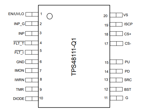
    I suppose the right way is to remove NC pins at all. For example TI made it with TPS48111-Q1 component (pin 16 is absent):

    But check me please. May be I miss something ...

    Best regards,

    Alex

  • Alex,

    I am not sure about this.  I see your point about conductive path of the pad eliminating that distances.  I will follow up.

  • Javier,

    I'm not sure too, but it makes me some sense.

    It is like lightnig strikes the upperst metal object, since the distanse from that point is closest to a cloud :) 

    I'll uppretiate for you update.

    Alex

  • Hello Alex,

    You are correct and you would need to use conformal coating to meet the IPC standard.  Sorry for not having another options.  You could use our isolation amplifiers which generally cost more or you could use our magnetic current sensors which will also have some limitations in current range and accuracy.=

    Regards,

    Javier

  • Hello Javier,

    Thanks for update.

    For future board I'll use SOIC package which has enough gap between pads.

    For VSSOP-10 package consider removing NC pins, so it will comply IPC. Otherwise there is no advantage of this package upon VSSOP-8, if you need covering with conformal coating. Conformal coating can solve the problem with SOT and with SSOP-8 as well.

    Good luck!

    Alex